Bacterial Imager Proposed

Petapixel, Phys.org: University of Exeter, UK students present a project called "Paint By COLI". The team attempt to modify E.coli bacteria with light sensitive and pigment production genes, in order to produce a full color biocamera. Bio-Photography is the application of genetically engineered bacteria to act as the light sensor of a camera, replacing digital sensors or photographic film. The surface area of bacteria is on the order of microns, so the resolution should be quite competitive with the current cameras. Individual bacteria functions would be geared for certain wavelengths — red light would stimulate production of cyan pigment, green light for magenta pigment and blue light for yellow.

The project is currently supported by The University of Exeter Annual Fund, CLES, CEMPS and academics from across the University. The group is going to present the project at the Genetically Engineered Machines (iGEM) event in Lyon, France on Oct. 11-13.

Crosstalk Reduction Between Multiple Structured Light Cameras

Microsoft Research posted its paper from CHI'12 conference "Shake’n’Sense: Reducing Interference for Overlapping Structured Light Depth Cameras" by Alex Butler, Shahram Izadi, Otmar Hilliges, David Molyneaux, Steve Hodges, and David Kim.


"The key behind Shake‟n‟Sense is to minimally vibrate a Kinect camera unit using an offset-weight vibration motor and thereby artificially introduce motion blur. Both the structured light DOE illuminator and the IR camera of the Kinect will move in harmony, which means that depth sensing works as normal, albeit with a little induced blur. However, even minor almost imperceptible motion of the sensor in this way causes blurring of structured light patterns from other units which serves to eliminate most of the crosstalk."

Update: It looks like University of North Carolina researchers proposed the same technique at about the same time.
Oppo is First to Use Tessera's MEMS AF

Oppo is First to Use Tessera's MEMS AF

Business Wire: Tessera's DigitalOptics Corporation (DOC) announces today that Guangdong Oppo Mobile Telecommunications Corp. has placed the first mems|cam volume production purchase order. "We are proud to announce that OPPO and DOC are exclusive launch partners. OPPO will be the first smartphone OEM to incorporate mems|cam products in volume," stated John Thode, president of DigitalOptics Corporation. "OPPO has an excellent premium brand in China as demonstrated by the September 23 launch of the innovative N1 Smartphone platform. Integrating mems|cam modules into OPPO’s best-in-class smartphones will bring an exciting computational imaging user experience that further delivers on OPPO’s brand promise."

There has been speculation on who would be the first to bring the significant benefits of mems|cam to the mobile imaging market. Last week, several technology news blogs reported that mems|cam was first being brought to market in another smartphone platform (Google Nexus 5). Those reports were inaccurate.

Forbes quotes China Morning Post publishing that Oppo's total production is expected to be about 15M phones this year.
European IR Sensor Industry Consolidates

European IR Sensor Industry Consolidates

Less than a year ago France-based Sofradir acquired Quantum Well-Infrared Photodetector (QWIP) and InGaAs sensor vendors. Now Sofradir and Onera announce an agreement to transfer Onera’s thermal imaging research group to Sofradir, together with a five-year project aimed at developing disruptive technologies in infrared detection in order to provide OEMs with more highly advanced capabilities in thermal imaging.

"Sofradir and Onera are collaborating once again to break down the technological barriers in infrared by exploring new possibilities in optical integration and other techniques," said Philippe Bensussan, chairman and CEO of Sofradir. "Onera is known for its vision, vast knowledge and expertise in aerospace and defense system design. We are excited about leading future developments in IR detection. We have high expectations about what these advantages will bring to our customers who design optronics systems for defense, space and commercial applications."

The project involves transferring emerging technologies and know-how from Onera, making them ready for industrial processing. The team will carry out research on and develop new techniques for infrared detectors, such as integrated optics, greater compactness, improved functionality and performance of thermal imaging equipment.

Silicon File and Dual Aperture to Cooperate on 3D Gesture Tracking Sensor

PRNewswire: Silicon File announces its collaboration with Dual Aperture, Inc., a Silicon Valley startup, to build a new type of CMOS image sensor that can take sharp pictures, significantly reduce noise, and capture real-time distance information. Furthermore, all of this is possible while utilizing a single, low-power, small form factor sensor instead of stereoscopic sensors, a common feature of most 3D cameras in the marketplace today.

Dual Aperture's image sensor technology relies on 4-color sensor design. The 4-color sensor is comprised of RGB and IR pixels, instead of the traditional Bayer pattern. The sensor uses two separate apertures, one for the RGB spectrum and the other for the IR spectrum, to simultaneously capture two distinct images with different sharpness levels.

Silicon File Technologies will incorporate Dual Aperture's 4-color sensor technology, related image processing algorithms, and various application software into their sensors and sensor module products. These technologies will enable the following features:

  • Reconstruction of color imaging from a 4-color pattern sensor
  • Noise reduction and image sharpening
  • Accurate depth estimation of objects captured in real-time
  • Real-time touch refocusing of pictures
  • Real-time 3D image pair generation
  • Accurate gesture tracking using a low-power, single sensor

"Dual Aperture's technology will enable new dimensions in photography with a multi-purpose camera that uses a low cost, low power, single CMOS image sensor," says Do Young Lee, CEO of Silicon File. "We are thrilled to be the first to partner with Dual Aperture in the growing market that Dual Aperture's 4-color sensor technology has created."
David D. Lee, CEO of Dual Aperture also adds that "Dual Aperture is looking forward to working closely with Silicon File Technologies to develop commercial products targeted for various platforms based on our new ideas and Silicon Files' strong design capabilities. Because of its small form factor and low power usage, Dual Aperture's 4-color sensor technology can be used in a variety of consumer devices, including smart phones, tablets, PCs, TVs and automobile applications."

Under the agreement, Silicon File and DA will work closely together to equip other camera OEMs with new multifunctional cameras. Silicon File will also manufacture and market 4-color sensors and camera modules integrated with new features enabled by DA algorithms.

Dual Aperture apparently does not have a web site. So far USPTO published two Dual Aperture's patent applications, while WIPO lists 7 applications filed in different countries.

Application US20130033579 named "Processing Multi-Aperture Image Data" shows details of the company's technology. The 3D depth imaging part of it is explained below:

Workshop on CMOS Image Sensors for High Performance Applications

Workshop on CMOS Image Sensors for High Performance Applications

CNES, ASTRIUM, THALES ALENIA SPACE, SODERN are organizers of the 3rd workshop "CMOS image sensors for high performance applications" to be held in Toulouse, France on November 26-27, 2013. The preliminary program includes:

CMOS sensors for space applications:
  • Nick Nelms, ESA
    An overview of ESA supported Visible and NIR CMOS Image Sensor development
  • Jérôme Pratlong, e2v
    MTG FCI Visible Detector design and development.
  • Weng-Lyang “Bill” Wang, CMOS Sensor Inc
    Five bands of CMOS Sensor (C468) for Formosat-5
  • Michel Bréart de Boisanger, EADS Astrium
    CMOS Image Sensors optimized for GEO observation
  • Fabien Malbet, IPAG
    Detector requirements for high accuracy astrometry and results of an interferometric detector calibration method
Low flux:
  • Franck Robert, Photonis
    Photonis complementary Digital Solutions for Low Light Level and extreme low light Vision conditions
  • Ajit Kumar Kalgi, Caeleste
    Photon imaging with monolithic CMOS SPADs
  • Alice Pelamatti, ISAE
    An Analytical Model for the Estimation of the Full Well Capacity in Pinned Photodiode CMOS Image Sensors
TDI on CMOS:
  • Alex Materne, CNES
    Development of Pixel architectures for TDI CMOS image sensors dedicated to High Resolution Earth Observation Satellites
  • Alper Ercan, IMEC
    A TDI test imager in embedded CCD in CMOS technology
  • Beat De Coi, ESPROS Photonics
    CCD/CMOS Imager System on a Chip
  • Olivier Marcelot, ISAE
    Study of CCD Transport on CMOS Imaging Technology: Comparison Between SCCD and BCCD, and Ramp Effect on the CTI
  • Frédéric Mayer, e2v
    Measurements and Analysis of a 13um Pitch Charge Transfer TDI Suitable for Space Applications Using a Standard CMOS Technology
ADCs:
  • Philippe Ayzac,Thalès Alenia Space
    Design of MROD, a Space Qualified, 2 Channel, Video Chain Mixed-Signal ASIC for High Resolution Mission
  • Daniel Dzahini, LPSC IN2P3
    TUTORIAL : SURVEY OF On-Chip ADCs FOR IMAGING APPLICATIONS
CMOS for Infra Red Applications:
  • Harald Weller, SELEX-ES
    IR Sensors for space and astronomy applications at Selex-ES Ltd
  • Vincent Gravot, ULIS
    A differential input stage for uncooled infrared pixels
  • Wim Vereecken, XENICS
    The design of a 1.3 Megapixel InGaAs array with low noise and increased dynamic range Backside Illuminated CMOS
  • Kiki Minoglou, IMEC
    Evaluation of backside passivation using laser annealing in backside illuminated image sensors
  • Jérôme Pratlong, e2v
    TAOS II: Three 88-Megapixel astronomy arrays of large area, backthinned, and low-noise CMOS sensors
  • Guy Meynants, CMOSIS
    Backside illuminated CMOS active pixel sensor with global shutter and 84 dB dynamic range
Radiation Hardness:
  • Manuel Innocent, ON Semiconductor
    A radiation tolerant 4T pixel for space applications: layout and process optimization
  • Harald Neubauer, IIS Fraunhofer
    Comparison of x-ray tolerant pixel-photodiode combinations (with and without in pixel charge-integration) for high sensitive x-ray detectors
  • Valerian Lalucca, ISAE
    Single Event Effects in 4T and 5T Pinned Photodiode CMOS Image Sensors
Thanks to CV for sending me the program. Registration for the workshop is open here.

Samsung Develops 13MP Camera Module with OIS

Tech-On reports that Samsung Electro-Mechanics has developed a 13MP camera module for smartphones featuring optical image stabilization. The OIS can correct angular errors up to 1.5deg. This is said to be better than digital cameras on the market usually correcting 0.7deg (Actually, best digital cameras correct up to 2-2.5deg - ISW).

The dimensions of the module are 10.5 x 10.5 x 5.9mm, similar the company's existing camera modules for smartphones. Samsung Electro-Mechanics is sampling of the camera module and negotiating with smartphone makers. The company plans to begin volume production in 1H 2014.

Sharp Introduces iSHCCD II and iSHartina

Sharp Introduces iSHCCD II and iSHartina

Sharp announces a pair of CCDs with PAL and NTSC resolutions, with improved IR sensitivity. The company also registered tow trademarks "iSHCCD II" and "iSHartina". "iSHCCD II" is said to be an advanced CCD that drastically improves light efficiency by including near infrared light region in a basic structure of "iSHCCD". The "iSHartina" series is said to be a key device group of Sharp which realizes a next-generation sensing world.
Google Buys Gesture Recognition Startup

Google Buys Gesture Recognition Startup

Gigaom, EETimes: Google has bought San Francisco-based gesture recognition startup Bot Square, developer of the Flutter. Flutter is an application that allows users to control media playback with simple gestures captured by their computer’s webcam. The company is said to be working on facial expression recognition to control mobile phones. There’s no word yet on financial details of the acquisition, but Flutter’s entire team of six employees, which includes four PhD’s, is said to join Google in Mountain View.
Rumor: Amazon Prepares 4-Camera Smartphone

Rumor: Amazon Prepares 4-Camera Smartphone

Techcrunch reports that Amazon Lab126 is in the process of developing smartphone with a 3D eye-tracking interface, one at each corner of the device. The cameras will be used to track eye and head motions in order to move the interface around to ‘give the impression’ of 3D picture on screen. Another feature said to be planned for the device, but not yet locked for release, is an image recognition feature that lets users take a shot of any real-world object and match it to an Amazon product for purchase. The new phone release is not planned for this year.

Omnivision's Shareholder Presentation

Omnivision has published its Sept. 26, 2013 shareholder presentation with the last year's results and plans for future:

Fujifilm Announces CMOS Sensor for Endoscopy

Fujifilm Announces CMOS Sensor for Endoscopy

In consumer applications this Fujufilm's announcement would sound like from 10 years ago. But medical market is different: "Fujifilm is proud to make use of the over-megapixel customised CMOS sensor. Our experience over many years in optoelectronics and electronic imaging shows the superior quality of this technology and we can expect that our customers will see the difference instantly" says Kazuhiko Takemura, Head of European Endoscope Department, Fujifilm Europe.

By adapting a CMOS image sensor, Fujifilm's 600 series endoscopes enable super-high resolution images to be produced. The leading-edge CMOS technology realizes less noise and brilliant images by converting the analog signal to digital in the tip of the scope. During transmission the digital signal is much less affected by any noise from the outside. CMOS technology also realizes 60fps progressive video.
Boyd Fowler Joins Google

Boyd Fowler Joins Google

Boyd Fowler's LinkedIn page shows that he's now Technical Program Manager at Google, since Sept. 2013. The page indicates that Boyd also continues his previous job at BAE Systems as Technical Director. Boyd has joined BAE through the acquisition of Fairchild Imaging where he was CTO. Boyd Fowler is one of the directors of IISS and recently was Co-Chair of IISW 2013 and the previous workshops too.

Pixpolar's Whitepaper

Pixpolar publishes a new technology page and a whitepaper discussing advantages of its MIG sensors's Non-Destructive Correlated Double Sampling NDCDS mode. One of the new capabilities of NDCDS is a possibility to choose ISO after the actual shot is taken in DSLRs:

"A great benefit of the MIG sensors is that the signal can be read-out accurately multiple times (due to Non-Destructive Correlated Double Sampling, NDCDS, ability). This means that one can provide the same image with multiple different ISO values. Thus one can either choose afterwards the best ISO setting or one can use different ISO values in different parts of the image. In the latter case the ISO value in each pixel is chosen e.g. such that the ISO is increased until the exposure value of the pixel exceeds a certain limit. This has also the unforeseen advantage that the amount of bits required in the Analog to Digital Converter (ADC) can be reduced while at the same time the Dynamic Range (DR) of the image can be improved.

If rolling shutter is utilized, which is typically the case in digital cameras, the reading of the signal multiple times with different ISO values bears the disadvantage that more skew is resulted in. However, in Digital Single Lens Reflex (DSLR) cameras mechanical shutter is typically used which means that the images are free of skew. Thus the MIG sensors offer for the DLSRs (and generally for digital cameras equipped with a mechanical shutter) a unique ability to afterwards adjust the ISO settings.
"

Another document on MIG sensors advantages for security applications shows the multiple NDCDS simulation results:

MIG Pixel

NIST Presents Passive THz Imager

Eureka: National Institute of Standards and Technology (NIST) have built a prototype passive THz imaging system for detecting hidden weapons and other threats at distances up to 28m away. The technology is similar to the NIST camera in the SCUBA-2 telescope in Hawaii. Both instruments detect emissions at a wavelength of 850um, a wavelength of light that passes through both clothing and the atmosphere. Both sets of sensor arrays are packaged with superconducting amplifiers to boost signal strength, using a NIST technique that makes large arrays practical. But the new imager's sensors are made of a different metal, aluminum, which superconducts at higher temperatures of 1.2 Kelvin. This allows the sensor array to be cooled by a more compact, custom refrigerator.

The NIST imager's video frame rate is currently 6fps, but NIST researchers say their system can be developed further to have four times as many sensors (for a total of 1,004), which would produce larger, near-full-body images at faster video frame rates. A short lab video demonstrating the imager will be available at NIST web site, when it opens again. Here is the older NIST presentation.

Meanwhile, the passive THz imaging seems to attract more and more attention. Other recent works include ones at Johnson C. Smith University at Charlotte, NC, and European THz imaging project commercialized by Spain-based Alfa Imaging:

Panasonic Wins Emmy Award for In-Camera Chromatic Aberration Compensation

Panasonic Wins Emmy Award for In-Camera Chromatic Aberration Compensation

Business Wire: Panasonic will be presented with a Technology and Engineering Emmy Award for 2013 by the National Academy of Television Arts & Sciences in recognition of the company’s development of In-Camera Electronic Compensation for Lateral Chromatic Aberrations in External Lenses. The trend to smaller imager formats and less-expensive optics had meant compromises in image performance without an alternative solution to this problem. The concept of modeling the aberrations of a lens and applying real-time electronic correction provides a very significant increase in image quality and permits lower cost-cameras and optics to create better images.

"Panasonic is honored to receive the coveted technical Emmy for its pioneering efforts in the development of Chromatic Aberration Compensation," said Michael Bergeron, Business Development Manager, Panasonic System Communications Company of North America (PSCNA). "This technology has helped us maintain high-quality imaging while making improvements in size, weight and affordability, and now combined with master-quality AVC-ULTRA recording and native 1920 x 1080 imagers, CAC has contributed to new benchmarks for HD acquisition, getting around inherent limitations of optics."
Forza Silicon to Present its BDA's FastSPICE-based Design Methodology

Forza Silicon to Present its BDA's FastSPICE-based Design Methodology

Business Wire: Daniel Van Blerkom, Forza Silicon CTO, and Ravi Subramanian, Berkeley Design Automation CEO, will jointly present a paper titled "An Efficient and Accurate Sign-Off Simulation Methodology for High-Performance CMOS Image Sensors" at the TSMC Open Innovation Platform Ecosystem Forum today in San Jose, CA. Forza Silicon uses the Analog FastSPICE (AFS) Platform from Berkeley Design Automation for circuit verification and sign-off validation of CMOS image sensors. The simulation methodology developed by Forza Silicon with the AFS Platform uses a hierarchy of models for the image sensor blocks. The complexity of the model is reduced at higher levels of the hierarchy, while still achieving maximum accuracy of the global interactions between blocks.

"With the ability to tailor our model complexity for a desired simulation, we gain the advantage of rapid, accurate validation while keeping simulation time and resources manageable," said Dr. Daniel Van Blerkom.

Teledyne DALSA Announces Full-Frame 32MP CCD Family

Teledyne DALSA releases a new FTF7046 family of full frame image sensors with 32MP. Using the latest 5.2um pixel, the company says it is able to preserve DR (>72dB linear), QE, and FF (>90%) in the FTF7046 even as they reduced pixel size to deliver 32MP in a 35mm optical format. The FTF7046 image sensors are available in color (RGB) and monochrome models. The sensor's frame rate is 1.2fps with 2 x 25MHz parallel outputs.

IHS: iPhone 5s Camera Gets Cheaper

Electronics360: Andrew Rassweiler, senior director of Teardown Analysis and Cost Benchmarking Service at IHS Electronics & Media, presented cost analysis of the new iPhone 5s and 5c, with both rear and front cameras taking roughly 6-7% of the BOM:

Preliminary Cost Estimate for iPhone 5s
Preliminary Cost Estimate for iPhone 5c

This is somewhat lower than IHS' last year estimation of $16.40 for the rear camera of iPhone 4s:

iPhone 4s Cost Analysis

Now I wonder how IHS came to the conclusion that iPhone 4S' 8MP 1.4um-pixel BSI camera module is cheaper than 5S' set of front and rear cameras 1.2MP+8MP, where the rear one has 1.5um pixel stacked sensor? Where do they find the savings? My guess is that they just estimated the chip areas, and, naturally, the stacked sensor came out smaller.
Sony Playstation 4 to Support Gesture Control

Sony Playstation 4 to Support Gesture Control

IGN, Forbes: At Tokyo Game Show, Sony confirmed the PlayStation 4 will support gesture control via the PlayStation Camera, similar to Xbox One’s Kinect. But while Kinect will come bundled with the console, Playstation 4 users will need to buy the optional gesture recognizing camera separately.
STMicro Develops B&W+R Sensor for Automotive

STMicro Develops B&W+R Sensor for Automotive

EETimes: STMicroelectronics develops B&W automotive image sensors for ADAS. An interesting feature is that it's able to single-out the red colored details, while everything else is B&W. When asked why red, ST BU director Martin Duncan said, "Red indicates a lot of important information - such as red traffic light, red road signs, brake lights, and tail lights."

Nokia Publishes More Lumia 1020 Camera Details

The official Nokia Conversations blog published few more 41MP Lumia 1020 camera details coming from Eero Salmelin, Nokia’s Head of Imaging:

"First we have the optics system with its six element lens, which... is the highest performing optics ever been put into a Nokia device."

"In Nokia’s OIS solution the whole lens system is resting on ball bearings. The special gyro components are very accurate and fast in detecting how the phone is moving and the lens is moved by the motors in the opposite direction very quickly to compensate for the handshake."

"The camera module is the casing that packages everything together so that it slots neatly inside the Lumia 1020. It measures 25mm by 17mm and contains well over 130 individual components. Every single camera component is tested, calibrated and the quality is verified. We make sure that each module performs extremely well."

Lumia 1020 camera module

Fujifilm and imec Develop New Photoresist for Organic Image Sensors

Fujifilm and imec have developed a new photoresist for organic semiconductors that enables the realization of submicron patterns and does not hurt the light sensitivity of the organic photodetectors. For technical verification, Fujifilm and imec developed organic photo detectors (OPD) using the new photolithography technology, and tested their performance. Organic semiconductor materials were patterned to produce OPD composed of fine light receiving elements down to 200μm×200μm size (for some reason marked as 300um x 300um on the graph below). Generally, patterning of organic semiconductor materials degrades the property of converting light into electricity, but the OPD developed in this case were patterned without degradation:

Organic semiconductor materials were patterned to form OPD
of 300μm×300μm size, and photoelectric conversion property
with irradiation of artificial sunlight (AM1.5G) (red dotted line)
was examined. When compared with photoelectric conversion
property without patterning organic semiconductor materials (red
solid line), it did not show degradation due to patterning.
Similarly, there was no difference between with patterning (black
dotted line) and without patterning (black solid line) for
unirradiated dark current.

Toshiba Announces Stereo 3D Depth-Enabled Camera Module

Business Wire: Toshiba announces what it says the industry’s first dual camera module for smartphones, tablets and mobile devices. TCM9518MD incorporates twin 1/4 inch optical format 5MP camera modules (5MP x 2 arrays) and simultaneously outputs recorded images and depth data. Images captured with the module can subsequently be manipulated to change the depth of field and point of focus. Samples will be available by January 2014, with mass production scheduled for April 2014.

The dedicated companion LSI of the “TCM9518MD” measures and appends depth data to objects in the image. These data can be used for a wide variety of applications, including focus and defocus, and even to extract and erase objects from the picture. Used in combination with customers’ applications, the module supports the creation of new functions.

The companion LSI generates 13MP images by upscaling images taken by the twin 5MP cameras, realizing a lower module height than that of conventional 13MP camera modules. The TCM9518MD brings high resolution and computational camera functionalities to the CMOS image sensor market for smartphones, tablets and mobile devices.

The pixel size is 1.4um and the camera module measures 8.0 x 12.0 x 4.65 mm according to the PR (or 18 (W) × 12 (D) × 4.65 (H) mm according to the company's product page):

LensVector Partners with Hosiden

LensVector Partners with Hosiden

Marketwired: LensVector and Hosiden announce an agreement for Hosiden to be LensVector's manufacturing partner. Production is scheduled to start early in 2014 in Hosiden's Shiga, Japan LCD facility. The agreement expands LensVector's manufacturing capabilities to serve the market for smartphones and other mobile devices. Hosiden will be using their LCD production technology, developed over a 40-year history of LCD production, to manufacture autofocus camera components to meet the quality and volume needs of the mobile phone market.

"Partnering with a world class manufacturer like Hosiden is an important step in establishing LensVector as the premier provider of solid-state autofocus lenses," said Howard Earhart, CEO, LensVector. "LensVector's manufacturing strategy is to merge high quality, low cost mature LCD panel manufacturing with our proprietary thin film process. This combination will provide very high capacity from existing Fabs yielding arrays of thousands of lens elements per panel."
Why There is No Camera Startups

Why There is No Camera Startups

Wired publishes an article by Marc Barros, the co-founder and former CEO of Contour, an action hands-free camera company. Marc discusses difficulties of creating a hardware company from scratch using camera startup as an example:

"Take cameras, for example. To make an amazing product you need: (1) a quality lens, (2) the latest image sensor, and (3) a powerful processor.

The best lenses are made in Japan (often by the camera makers themselves), so access to these components begins with $500K up front in engineering services and a guaranteed minimum order well into the thousands. Meanwhile image sensor companies are quickly being consolidated — so if a purchasing company isn’t a big name, it can’t even get access to the good stuff. For processors at least, the U.S. companies who created them are willing to provide access (to their true roadmap, SDK documentation, and engineering services), because they understand the importance of helping entrepreneurs build a product that maximizes their platform.

Overall, however, this lack of components means a hardware startup has to build volume with a crappy camera before they can make a really good one.

And of course, the established hardware players know their advantage in components is a massive barrier to entry. A few of them, like Sony and Samsung, are willing to sell other companies the same components used in their products as long as they don’t directly compete with them. Other companies, like Canon, build their own components to get ahead of the competition.
"

TSMC Develops Hardmask for Deep Implants

TSMC is going to present its recent developments in hardmask for deep implants in small pixel sensors at NMDC, Taiwan on Oct 6-9, 2013. The paper is titled "Nanotechnology Development for CMOS Image Sensor Applications" by C.C. Wang, T.H. Hsu, S.F. Ting, C.Y. Chen, K.C. Huang, J.C. Liu, S. G. Wuu. TSMC has developed a nice hardmask process for pixel size of order of 1um:

imec Presents its Image Sensor Technology

Samsung Announces ISOCELL Pixel Technology

Business Wire: Samsung announces its new pixel technology, ISOCELL. "This new technology substantially increases light sensitivity and effectively controls the absorption of electrons [I'd guess they meant collection of electrons], resulting in higher color fidelity even in poor lighting conditions."

"Previous sensor technology developments focused on improving the light absorption of each pixel, and have progressed pixel technology from FSI (Front Side Illumination) to BSI (Back Side Illumination) which places photodiode at the top to maximize photoelectric efficiency. While being very effective at the time, this BSI technology also faced limitations in improving image quality as pixel sizes continued to decrease.

Building on these past advances and continuing the push toward higher quality image sensors for mobile devices, Samsung has developed ISOCELL the next generation of pixel technology, which is patent pending. ISOCELL technology forms a physical barrier between neighboring pixels – isolating the pixel. This isolation enables more photons to be collected from the micro-lens and absorbed into the correct pixel’s photodiode minimizing undesired electrical crosstalk between pixels and allowing expanded full well capacity (FWC).

Compared to conventional BSI pixels, the ISOCELL pixels decrease the crosstalk by approximately 30 percent which results in higher color fidelity to reproduce the original color with sharpness and richness, and increase the full well capacity (FWC) by 30 percent which leads to greater dynamic range.

Additionally, an imager designed with ISOCELL can feature a 20 percent wider chief ray angle (CRA), reducing the height of the camera module. This makes it suitable for slim and small form factor mobile devices with challenging low z-height requirements.

As the first Samsung image sensor to adopt this new technology, the S5K4H5YB 8Megapixel imager utilizes a 1.12um ISOCELL pixel and has a 1/4inch optical format. The S5K4H5YB is currently sampling to customers with mass production scheduled for Q4 2013.

According to market research firm Techno System Research, in 2014, approximately 66 percent of smartphones will feature image sensors with 8Mp or higher resolution.
"

Samsung Tomorrow, the official Samsung blog, publishes ISOCELL vs BSI comparison picture (click to expand):

IR on Aliasing Artifacts

Imaging Resource posted an interesting note on the recent trend to remove optical low pass filters over the sensors:

"There's been a strong move in the camera industry lately to remove low-pass filters (aka anti-aliasing filters or LPFs) from cameras, in pursuit of greater image sharpness... At IR, we feel strongly that eliminating low-pass filters is a bad idea, and a mistake for the industry. While the vast majority of natural subjects aren't subject to aliasing and moiré issues, many man-made objects have the sort of regular patterns that trigger the problem."

Imaging Resource supports its claim by real-world examples shot by one of the recent cameras with no optical anti-aliasing filter:

Example of color aliasing, caused by the fine thread patterns in the model's outfit.
Example of luminance moiré in the form of the swirly lines
in what should be diagonal louvers on the building's front.

Pelican Imaging Publishes Full Resolution Original Images

Pelican Imaging publishes its oncoming paper at SIGGRAPH Asia 2013, including many high resolution images straight out of their reference system:

PiCam: An Ultra-Thin High Performance Monolithic Camera Array
Kartik Venkataraman, Dan Lelescu, Jacques Duparré, Andrew McMahon, Gabriel Molina, Priyam Chatterjee, Robert Mullis, and Shree Nayar

The full resolution pictures on Pelican's site are 3264 x 2448 and over 30MB in size, too large to post here. A down-scaled version of 1000 x 750 and full resolution crop of one of the images are below:


There are many more original images on the Pelican site, including ones taken at 30-50lux/15fps and 5-10lux/7fps ones. It's quite rare that an image sensor manufacturer posts the official full-resolution samples, including ones shot in the difficult lighting conditions.

An official press release is expected tomorrow. Thanks to LG for giving me a heads-up!

Update: The official PR is published on PRNewswire now.
Mike Tompsett's Presentation

IISW 2013 page publishes the presentation slides of Mike Tompsett, the inventor of the first CCD imager. The presentation slides talk about the early solid state imager history and more.


Thanks to EF for letting me know!

iFixIt: iPhone 5S Sensor Probably Made by Sony

iFixit team teared down the new Apple iPhone 5S. The conclusion regarding the main camera is:
  • We uncover the iSight camera.
  • The back of the iSight camera is labeled DNL333 41WGRF 4W61W.
  • According to our good friend Jim Morrison, Vice President of the Technology Analysis Group at Chipworks, "the DNL markings are consistent with the markings on the camera modules housing the Sony IMX145 we saw in the iPhone 4s and on the iPhone 5. The marks on the side of the module are different, but our industry insiders tell us this is Sony's again"
  • As Apple has stated the pixel pitch on this camera is 1.5 µ, this sensor should not be the IMX145, but a newer variant.


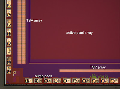
Update: Chipworks reverse engineering confirmed Sony sensor inside iPhone 5s camera. It's a stacked sensor:

IHS Predicts Fast Growth in Automotive Gesture Recognition Systems

IHS forecasts that the global market for automotive proximity and gesture recognition systems to control in-car infotainment with a simple wave of their hand will grow to more than 38M units in 2023, up from about 700,000 in 2013. Nearly 40% of all new automobiles sold worldwide in 2023 will come with some degree of proximity or gesture recognition, according to a new IHS Automotive report entitled "Emerging Technologies: New Human-Machine Interface Trends."

Gesture recognition is defined as the use of cameras or sensors to track and convert a user’s movements into inputs for the infotainment system without any physical touch input. This would include things like waving a hand to the left or right to change radio presets or go to the next song in a playlist, or turning the hand clockwise or counterclockwise to raise or lower the volume.

A*STAR IME and nanoX Imaging to Develop MEMS X-ray Imager

A*STAR IME and nanoX Imaging to Develop MEMS X-ray Imager

Singapore A*STAR's Institute of Microelectronics (IME) and Japan-Israel-USA startup nanoX Imaging are to jointly develop a MEMS X-ray imager based on field emission detection. "We are confident that that the partnership with IME will be long-standing. In this first collaboration, we look forward to present to the medical industry an ideal solution of an imaging system that will offer high performance at low radiation risks," said Hitoshi Masuya, CEO of nanoX Imaging.

OMRON to Launch Imaging System for Interpretation of People's Intentions and Conditions

OMRON announces its Human Vision Component (HVC), a new image sensing component that can be embedded in a variety of devices and equipment. The HVC integrates ten algorithms from OKAO Vision and a camera module to a system capable of recognizing the intentions and conditions of people through face recognition, estimation of facial expressions, age estimation, gaze estimation, hand detection, and other functions. Launch of the standard-type HVC is scheduled for December. From next year onward, OMRON plans to introduce a succession of application-specific HVC products, which will incorporate optimized hardware and optical systems to enable customized functions that meet the requirements of each specific industry.

Examples applications include air conditioners capable of automatically adjusting the temperature to the level that people feel most comfortable; lighting products with efficient automatic control depending on the presence of people, their movements, or other conditions; automatic vending machines that suggest a product that matches the preference of a specific consumer; home appliances controllable via hand movements; robots that can react to the facial expressions of users; cars that prevent drowsy or inattentive driving by recognizing signs of fatigue in the driver's face; and more.

The ten functions to recognize the intentions and conditions of people are:
  1. face detection
  2. human body detection
  3. gender estimation
  4. age estimation
  5. gaze estimation
  6. facial pose estimation
  7. face recognition
  8. estimation of facial expressions (satisfied, unsatisfied, five different expressions: happiness, surprise, anger, sadness, and neutral)
  9. hand detection
  10. blink estimation
Adimec on Smaller Pixels in Security

Adimec on Smaller Pixels in Security

Adimec blog's recent post discusses the benefits and issues of using smartphone-style small pixels in 24/7 security camera applications. The pros and cons of small pixels are:

Pros:
  • Lower costs and weight through smaller sensors, optics, and cameras
  • Increased resolution with same sensor size and optics
  • Sensitivity in dim light is acceptable
  • Color reproduction can be good enough

Cons:
  • Give up global shutter (get rolling shutter)
  • Slower frame rates
  • More noise
  • Lower full well capacity
  • Lower MTF
  • Optical/Electrical crosstalk
  • Lower quality available optics

Thanks to GA for the link!

Truesense Publishes Detailed Spec of its First CMOS Sensor

Truesense Imaging has published a detailed 51-page spec of its first CMOS sensor KAC-12040, including QE, angular response and pretty much everything else one can think of. I believe Truesense's spec together with ON Semi's are the most detailed image sensor specs that are openly available on the net:

Truesense Announces Production Start of Fast CMOS and CCD Sensors

Truesense Imaging announces that its 12MP/70fps, 4.7um pixel KAC-12040 CMOS sensor, and 7.4um pixel based 1080p60 KAI-02170 and 4MP/28fps KAI-04070 Interline CCDs have now been released for production. "Through their features, functionality, and performance, these new products demonstrate the complementary nature of CCD and CMOS devices, and show the importance of having both technologies available in a full-featured product portfolio," said Chris McNiffe, CEO of Truesense Imaging.

The company has published a brief spec of its first CMOS sensor based on 5T GS pixels and said that it's the first of the future family:

Canon Captures Firefies 30fps Video at its Full-Frame DSLR Sensor

Canon announces that it was able to capture a video of Yaeyama-hime fireflies flying in darkness on the high-sensitivity 35 mm full-frame CMOS sensor with 19um pixels developed by the company for video capture and announced in March 2013. No artificial lighting was used during shooting, which took place after sunset amid the island's mountains. Despite an exceptionally dark shooting environment of less than 0.01 lux, a level in which the naked eye would have difficulty discerning surrounding objects, the CMOS sensor at 30fps was able to capture not only the color of the light emitted by the fireflies, each of which measures only a few millimeters in length, and their movements, but also the surrounding vegetation in which the species lives.

Yaeyama-hime fireflies amid jungle vegetation
(Photomontage created from video footage)

A Youtube copy of the video from Canon site shows the footage:


PC Magazine Reviews Image Sensor Technology

PC Magazine Reviews Image Sensor Technology

PC Magazine published a surprisingly big and complete, albeit popular, review of image sensors history, principles, and technology. The 10-page article spans from film to CCD and CMOS sensors, from doping types to pn-junctions to process and then to packaging. Overall, it gives quite a complete picture for beginners.

Oops, the article is dated by 2001, quite old.
Movidius on Future of Imaging

Movidius on Future of Imaging

Wired: Movidius CEO Remi El-Ouazzane publishes an article on future technologies in mobile imaging. The main points are:
  • Always-On Mobile Computer Vision Systems Coming Soon
  • Advanced camera topologies and novel image sensors; specifically lightfield cameras and array cameras.
  • Depth-enabled applications: enable next-generation applications such as Bokeh effects; background substitution in video conferencing; computational refocusing; improved gesture recognition; and image relighting using depth.
  • HDR video. A key element of HDR still imaging and video is to compress the dynamic range using tone mapping.
  • Stereo 3D imaging.
  • Simultaneous localization and mapping (SLAM): Mobile applications take advantage of the SLAM capability to map and navigate in complex unknown indoor environments.
  • Eulerian video magnification to reveal hidden information. All manner of micro changes in video streams to be magnified and observed, from the flow of blood as it fills the face to the movement of babies.
  • Sensor metadata: For example, multiple sensors (microphone, GPS, accelerometer, compass, etc.) can augment the cameras while network can supply rich semantic information

Thanks to DM for the link!
IntoPix Presents TICO Light Video Compresion

IntoPix Presents TICO Light Video Compresion

Belgium-based IntoPix presents TICO - "visually lossless light compression specifically designed for the industry. This revolutionary technology is extremely tiny in hardware (FPGA, ASIC) , fast and powerful in software (CPU), robust for real-time operation with no latency." TICO is said to be "a smart upgrade path to manage higher resolutions (4K, 8K…) and frame rates while assuring visual quality, keeping power and bandwidth at a reasonable budget and reducing significantly the complexity and cost of the system." It features:
  • Visually Lossless quality between 2:1 and 4:1.
  • Persistent and Robust: Indistinguishable image loss over multiple generations
  • Latency: Few Microseconds – very few line of pixels ( selectable from 1 to x)
  • Small complexity and compact codec: easy to implement in low-cost FPGA or ASIC. It uses little internal memory and no external memory.
  • Powerful , Real-time or faster than real-time in CPU
  • Compatible with different resolutions, from mobile to 4K/8K UHDTV, via multiple usual transport schemes.
  • Designed to be a standard for the industry-wide support: TICO compression technology is available on multiple software and hardware technologies.

SiOnyx Shows 1mlux Imaging

Vision System Design: SiOnyx has shown its IR sensors at this year's SPIE Defense and Security Symposium in Baltimore, MD:

Comparison at below 1 mLux for a Best in Class CCD (left)
and SiOnyx XQE-1310 1.3MP 10um pixel imager (right).

According to Dr. Martin Pralle, VP of Business Development at SiOnyx, all the XQE sensors feature a 72dB native DR and an on-chip HDR feature that allows up to 120dB DR to be achieved. To date, the company has not yet openly published the spectral characteristics of these devices but, Pralle says. All Pralle would say was that at approximately 1064nm, the devices exhibited a QE approximately ten times that of standard CMOS image sensors. For night-vision applications, the US Army recently tested the SiOnyx XQE-1310 sensor in its labs and confirmed imaging at 1 mLux (1×10-4 Ft-candles).