AutoSens 2016 kindly permitted me to post a couple of slides from Softkinetic presentation "3D depth-sensing for automotive: bringing awareness to the next generation of (autonomous) vehicles" by Daniel Van Nieuwenhove. A good part of the presentation compares ToF with active and passive stereo solutions:
Samsung System LSI Might Split into Fabless and Foundry Businesses
According to BusinessKorea sources, Samsung is contemplating to split its semiconductor business into a fabless and foundry divisions:
"Samsung Electronics’ System LSI business division is largely divided into four segments; system on chip (SoC) team which develops mobile APs, LSI development team, which designs display driver chips and camera sensors, foundry business team and support team. According to many officials in the industry, Samsung Electronics is now considering forming the fabless division by uniting the SoC and LSI development teams and separating from the foundry business."
"Samsung Electronics’ System LSI business division is largely divided into four segments; system on chip (SoC) team which develops mobile APs, LSI development team, which designs display driver chips and camera sensors, foundry business team and support team. According to many officials in the industry, Samsung Electronics is now considering forming the fabless division by uniting the SoC and LSI development teams and separating from the foundry business."
Nikon Applies for 2-Layer Stacked PDAF Patent
NikonRumors quotes Egami talking about Nikon patent application with 2-layered pixel array forming a cross-type PDAF: "Nikon patent application is to use the two imaging elements having different phase difference detection direction in order to achieve a cross-type AF."
Thanks to TG for the link!
Thanks to TG for the link!
Sony, ON Semi Image Sensor Innovations
Framos publishes interviews with Framos North America VP Sebastian Dignard and ON Semi Go To Market Manager Michael DeLuca on image sensor innovations:
Edoardo Charbon and Junichi Nakamura Elevated to IEEE Fellows
Edoardo Charbon and Junichi Nakamura has been elevated to IEEE Fellows. Thanks to AT for the info!
More on Hitachi Lensless Camera
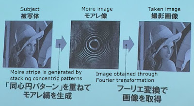
Nikkei publishes an article with more details on Hitachi lens-less camera:
"In general, the method that Hitachi employed for its lens-less camera uses a "moire stripe" that can be obtained by stacking two concentric-patterned films with a certain interval and transmitting light through them. The numerous light-emitting points constituting the image influence the pitch and orientation of the moire stripe. The location of light, etc can be restored by applying two-dimensional Fourier transformation to the moire stripe.
This time, Hitachi replaced one of the films (one that is closer to the image sensor) with image processing. In other words, one film is placed with an interval of about 1mm, but the other film does not actually exist. And, instead of using the second film, a concentric pattern is superimposed on image data."
Image Sensors at ISSCC 2017
ISSCC publishes its 2017 advance program. Sony is going to present its 3-die stacked sensor, a somewhat expected evolution of the stacking technology:
A 1/2.3in 20Mpixel 3-Layer Stacked CMOS Image Sensor with DRAM
T. Haruta, T. Nakajima, J. Hashizume, T. Umebayashi, H. Takahashi, K. Taniguchi, M. Kuroda, H. Sumihiro, K. Enoki, T. Yamasaki, K. Ikezawa, A. Kitahara, M. Zen, M. Oyama, H. Koga, H. Tsugawa, T. Ogita, T. Nagano, S. Takano, T. Nomoto
Sony Semiconductor Solutions, Atsugi, Japan
Sony Semiconductor Manufacturing, Atsugi, Japan
Sony LSI Design, Atsugi, Japan
Canon presents, apparently, a version of its IEDM global shutter sensor paper with more emphasis on the readout architecture:
A 1.8erms Temporal Noise Over 110dB Dynamic Range 3.4μm Pixel Pitch Global Shutter CMOS Image Sensor with Dual-Gain Amplifiers, SS-ADC and Multiple-Accumulation Shutter
M. Kobayashi, Y. Onuki, K. Kawabata, H. Sekine, T. Tsuboi, Y. Matsuno, H. Takahashi, T. Koizumi, K. Sakurai, H. Yuzurihara, S. Inoue, T. Ichikawa
Canon, Kanagawa, Japan
Other nice papers in the Imager session are listed below:
A 640×480 Dynamic Vision Sensor with a 9μm Pixel and 300Meps Address-Event Representation
B. Son, Y. Suh, S. Kim, H. Jung, J-S. Kim, C. Shin, K. Park, K. Lee, J. Park, J. Woo, Y. Roh, H. Lee, Y. Wang, I. Ovsiannikov, H. Ryu
Samsung Advanced Institute of Technology, Suwon, Korea;
Samsung Electronics, Pasadena, CA
A Fully Integrated CMOS Fluorescence Biochip for Multiplex Polymerase Chain-Reaction (PCR) Processes
A. Hassibi, R. Singh, A. Manickam, R. Sinha, B. Kuimelis, S. Bolouki, P. Naraghi-Arani, K. Johnson, M. McDermott, N. Wood, P. Savalia, N. Gamini
InSilixa, Sunnyvale, CA
A Programmable Sub-Nanosecond Time-Gated 4-Tap Lock-In Pixel CMOS Image Sensor for Real-Time Fluorescence Lifetime Imaging Microscopy
M-W. Seo, Y. Shirakawa, Y. Masuda, Y. Kawata, K. Kagawa, K. Yasutomi, S. Kawahito
Shizuoka University, Hamamatsu, Japan
A Sub-nW 80mlx-to-1.26Mlx Self-Referencing Light-to-Digital Converter with AlGaAs Photodiode
W. Lim, D. Sylvester, D. Blaauw
University of Michigan, Ann Arbor, MI
A 2.1Mpixel Organic-Film Stacked RGB-IR Image Sensor with Electrically Controllable IR Sensitivity
S. Machida, S. Shishido, T. Tokuhara, M. Yanagida, T. Yamada, M. Izuchi, Y. Sato, Y. Miyake, M. Nakata, M. Murakami, M. Harada, Y. Inoue
Panasonic, Osaka, Japan
A 0.44erms Read-Noise 32fps 0.5Mpixel High-Sensitivity RG-Less-Pixel CMOS Image Sensor Using Bootstrapping Reset
M-W. Seo, T. Wang, S-W. Jun, T. Akahori, S. Kawahito
Shizuoka University, Hamamatsu, Japan;
Brookman Technology, Hamamatsu, Japan
A 1ms High-Speed Vision Chip with 3D-Stacked 140GOPS ColumnParallel PEs for Spatio-Temporal Image Processing
T. Yamazaki, H. Katayama, S. Uehara, A. Nose, M. Kobayashi, S. Shida, M. Odahara, K. Takamiya, Y. Hisamatsu, S. Matsumoto, L. Miyashita, Y. Watanabe, T. Izawa, Y. Muramatsu, M. Ishikawa;
Sony Semiconductor Solutions, Atsugi, Japan;
Sony LSI Design, Atsugi, Japan
University of Tokyo, Bunkyo, Japan
The tutorials day includes one on deep learning processors:
Energy-Efficient Processors for Deep Learning
Marian Verhelst
KU Leuven, Heverlee, Belgium
Basler's First ToF Camera Enters Series Production
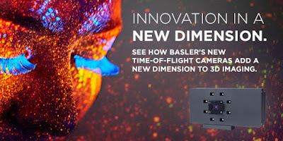
Basler: After a successful conclusion of the evaluation phase and extremely positive customer feedback, Basler first ToF camera is now entering series production. The VGA ToF camera is said to stand out for its combination of high resolution and powerful features at a very attractive price. This outstanding price/performance ratio puts the Basler ToF camera in a unique position on the market and distinguishes it significantly from competitors' cameras.
The Basler ToF camera operates on the pulsed time-of-flight principle. It is outfitted with eight high-power LEDs working in the NIR range, and generates 2D and 3D data in one shot with a multipart image, comprised of range, intensity and confidence maps. It delivers distance values in a working range from 0 to 13.3 meters at 20fps. The measurement accuracy of the Basler ToF camera is +/-1 cm at a range from 0.5 to 5.8 meters, while consuming 15W of power.
The Basler ToF camera operates on the pulsed time-of-flight principle. It is outfitted with eight high-power LEDs working in the NIR range, and generates 2D and 3D data in one shot with a multipart image, comprised of range, intensity and confidence maps. It delivers distance values in a working range from 0 to 13.3 meters at 20fps. The measurement accuracy of the Basler ToF camera is +/-1 cm at a range from 0.5 to 5.8 meters, while consuming 15W of power.
Movidius on IoT Vision Applications
ARMDevices interviews Movidius VP Marketing, Gary Brown, on the company low power advantages of their vision processor in different applications:
Jaroslav Hynecek Gets 2016 EDS J.J. Ebers Award
IEEE Electron Devices Society publishes a list of this year's awards. Jaroslav Hynecek receives 2016 EDS J.J. Ebers Award for "For the pioneering work and advancement of CCD and CMOS image sensor technologies." The Award is to be presented at IEDM in December.
Subscribe to:
Posts (Atom)


