Mantis Vision's CTO, Gur Bittan presents "Mobile Depth Sensing Methods and What They're Good For" at GPU Technology Conference held in March 2014. One can download the presentation video here or see it below.
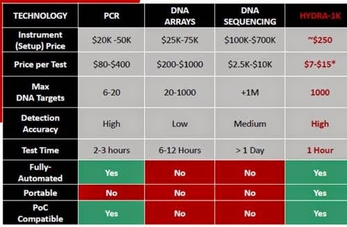
InSilixa Presents DNA Testing Sensor
EETimes: InSilixa comes out of stealth mode with a promise to deliver a cheap DNA testing technology PCR by means of 32 x 32 image sensor array. The sensor is supposed to cost $20-$50, has 100um pixel pitch and is manufactured in IBM 250nm process:

In 2013, the startup company won Nokia XCHALLENGE award, as seen in this Youtube video:
In 2013, the startup company won Nokia XCHALLENGE award, as seen in this Youtube video:
Olympus Proposes 2-Layer RGB-IR Sensor
Egami blog publishes Olympus Japanese patent application 2014-135535 proposing a 2-layer RGB-IR sensor. The main purpose is to remove the need in IR-cut filter.

iFixit Reveals Mantis Vision 3D Camera inside Google Project Tango Tablet
iFixit teardown shows that Mantis Vision structured light camera is responsible for Google Project Tango tablet 3D vision. The teardown team quotes Google: "The IR projector is from Mantis Vision, and designed specific to our specs for field of view and resolution. It is custom designed to work in partnership with the 4MP RGB-IR camera on the other side."


ON Semi Defines Post-Acquisition Aptina Organization
Business Wire: ON Semiconductor announces the completion of its acquisition of Aptina Imaging. ON expects to establish a new reporting segment, which will incorporate the financial results of the company’s consolidated sensor businesses, including the recent acquisitions of Aptina Imaging and Truesense Imaging, and ON Semiconductor’s existing optical, image and touch sensor businesses. The company expects to begin reporting financial results for the newly created segment from Q3 2014.
Taner Ozcelik, has been named SVP of the Aptina image sensor business and will report to Keith Jackson, president and CEO of ON Semi. Before the acquisition, Taner Ozcelik used to be Aptina SVP responsible for the Automotive and Embedded business.
For the Q3 2014, the acquisition of Aptina will likely contribute revenue in the range of $60M to $70M. Excluding the costs related to restructuring, and other acquisition related items, the acquisition of Aptina is expected to be slightly accretive to the ON's non-GAAP net income in Q3 2014.
In its investor presentation, ON Semi shows financial targets for Aptina business:

ESPROS Improves its ToF Evaluation Kit
Espros Photonics presents an improved version of the evaluation kit for its epc610 ToF sensor:

"The new epc610 Evaluation Kit is a significant upgrade from the former version. We opted for a completely new hardware design of the camera module. This module is based on our thorough background on TOF and incorporates the recent learnings from our customers.
A first novelty is an LED subsystem, which is optimized to illuminate the operation range in a more uniform way. Seven LEDs (Osram SFH 4059) are placed at the edge of the camera PCB. These LEDs cover the more distant operating range. Together, they deliver a high intensity, but due to the placement away from the receiver lens, their effect drops drastically at close range. This is where the single short range LED jumps in. Placed close to the receiver lens this single LED is much better suited to delivering light on to close objects, while its effect fades when the targets move further away. The result of this design is an illumination intensity with reduced peaks at certain distances. On signal level, this translates to a lower dynamic range that needs to be covered by the the detector system. Ask your sensor specialist and he will tell you why he likes that! With this design, the epc610 Camera Module works in a range from zero up to about three meters – depending on the target reflectivity."
Taiwan LIPS Presents ToF Stereo 3D Camera
As written in comments to the previous post, Taiwan-based LIPS posted Youtube videos demoing a 3D camera based on combination of ToF and stereo. No explanation of the technology is given, other than saying it's compatible with Primesense openNI 1.5 and 2.x software.
Richard Crisp on 3D Imaging
Image Sensors Americas conference publishes an interview with Richard Crisp from Etron on future of 3D imaging. Few quotes:
"I see the key applications in the area of control, security, visualization and reproduction. Significant market opportunities lie ahead in general-purpose computing/communications platforms (notebook/tablet/smartphone) as well as in fixed function appliances."
"The area of end application concepts, software and infrastructure are major areas of activity today. Once fully deployed, the impact of 3D imaging technology on our everyday life will be transformative in the same way the internet was: it will fundamentally change how we do things."
IMEC CMOS Imagers with Embedded CCD
Sensors Online published IMEC's Piet De Moor article "CMOS Imagers with Embedded CCD." Few quotes:
"Imec developed a CMOS compatible CCD module and included this into its custom imager 130-nm process... Imec implemented a number of process modifications to realize a CMOS compatible CCD module in its 130-nm custom image sensor technology platform. The embedded CCD module uses a single layer poly-silicon CCD electrode with narrow gaps to allow efficient charge transfer. It is customizable depending on application needs, and is compatible with back-side illumination."
"Embedded CCD, being a CCD compatible with CMOS operating voltages, opens possibilities for new and rich pixel architectures. For example, users could utilize an in-pixel CCD to implement a charge-domain global shutter functionality. Although this concept to image a full frame at the same exact timing is possible using CMOS imagers, it generally comes with a noise penalty.
Other possible uses of embedded CCD pixels include extreme high-frame rate burst imagers, where subsequent frames are stored inside the pixel using small CCD based analog memories. Certain time-of-flight implementations could also benefit from this technology. In addition to monolithic TDI applications for industrial inspection, TDI functionality is also used in hybrid infrared and x-ray imagers."
Aptina Shipped 50M Automotive Sensors in 10 Years
Aptina has shipped 50 millionth image sensor for automotive systems. The company estimates that nearly one in every two cars with an imaging solution uses an Aptina image sensor. The company sees this as an important milestone in its ten years of focus on automotive imaging.
Nikkei: Sony Aims to Capture 50% of Automotive Sensor Market, Prepares Sensor with 10x Sensitivity
Nikkei says that Sony has developed a sensor for automotive applications, which is "10 times as sensitive to light as existing chips, allowing for easier detection of objects in dark environments. The sensor can provide a color display of the surrounding area even in moonlight, enabling it to detect obstacles more readily than a driver can." Sony plans to start mass production of the sensor and begin sales to automotive equipment manufacturers in the latter half of 2015. The new sensor is expected to appear in car-mounted devices in 2016.
Aptina and OmniVision are leading the automotive image sensor market now. "But Sony aims to eventually pick up 50% of the market." Annual production of smart cars equipped with many cameras is expected to reach 100 million vehicles by 2025.
Aptina and OmniVision are leading the automotive image sensor market now. "But Sony aims to eventually pick up 50% of the market." Annual production of smart cars equipped with many cameras is expected to reach 100 million vehicles by 2025.
Omnivision Gets $1.64B Takeover Offer
Fox Business News, Seeking Alpha, WSJ, Barron's: Omnivision says it received a $1.64 billion takeover offer from a Chinese investor group led by Hua Capital Management Ltd. The investor group includes state-owned Shanghai Pudong Science and Technology Investment Co. Omnivision's board is reviewing Hua's proposal, and has made no decision yet.
Update: Here is the official Omnivision statement on the offer.
Update: Here is the official Omnivision statement on the offer.
4.4 Tera-fps Camera
Nature Photonics publishes a paper from a number Japanese universities and research centers showing 450x450 pixel imaging at 4.4 trillion fps:
"Sequentially timed all-optical mapping photography (STAMP)"
K. Nakagawa, A. Iwasaki, Y. Oishi, R. Horisaki, A. Tsukamoto, A. Nakamura, K. Hirosawa, H. Liao, T. Ushida, K. Goda, F. Kannari & I. Sakuma
The paper is supplemented by a nice videos explaining the camera operation and showing the demo movies (see more videos at the bottom of the Nature Photonics page):
Image Sensors in HVAC System
Why would HVAC system need an image sensor? Trane International's patent application US20140217185 "HVAC System With Camera and Microphone" by Kirby Neal Bicknell explains that the right question is not "why" but "how many image sensors":
"An image data set captured by the image sensor or an audio file captured by the microphone may be searched for the presence of predetermined conditions to reconfigure user settings. For example, if User A likes the room kept at 65 degrees in the winter, while User B likes the room kept at 72 degrees in the winter, an HVAC controller may recognize the presence of either User A or User B to change the default settings to the preferences of that particular user. In addition, the HVAC system controller may be programmed to prioritize one user over another user.
In another example, an HVAC system may be configured to cool a house when the temperature rises above 72 degrees. However, if an image sensor attached to an outdoor unit captures an image of User C or User D in the back yard, the HVAC system may override the default settings and suppress the cooling operation until User C and/or User D leave the back yard. This may be done to suppress the noise generation by the outdoor unit, or for various safety considerations. If User C is a small child, the operation of the outdoor unit with a high speed fan may present a safety consideration. If User D is typically present to mow the yard, presence of this individual may be a condition to trigger shut down of the outdoor unit to avoid grass being sucked into the outdoor unit, and clogging the heat exchanger."
Image Sensor Americas Interviews
Image Sensor Americas conference publishes tow new interviews on its site. Forza Silicon CTO Daniel Van Blerkom talks about image sensor design:
"Backside illuminated technology (BSI) is now becoming standard, even in custom sensors. This, coupled with 3D packaging with dense interconnects, is creating an exciting opportunity in stacked sensors. We are currently working on projects utilizing pixel level interconnects in 3D stacked devices."
"Forza Silicon team is in the process of developing a compact, low-power 3D sensor technology that can enable a wide range of smart applications in the programmable world (otherwise know as the "Internet of Things")."
IMEC image sensor group manager Piet De Moor too talks about stacked sensor technology:
"I expect a big impact of stacked image sensors, not so much on the image sensing quality but rather at the system integration level, which will enable smart and very compact imagers for both consumer (e.g. mobile phone) as industrial inspection and security imaging systems."
"The additional functionality offered by stacking is the potential of an area distributed pixel readout right underneath the pixel area, which allows a very fast or high dynamic range readout, a local analog-to-digital conversion, local image processing or combinations of above."
Aptina Announces Automotive SoC with De-Warp Functionality
Business Wire: Aptina is in mass production of the ASX344AT SOC for backup cameras. The 1/4-inch, 5.6um pixel VGA resolution ASX344AT delivers 180 degree viewing with de-warp functionality. The National Highway Traffic Safety Administration (NHTSA) found that 180 degree camera solutions provide a nearly 60% improvement over traditional mirror-based systems and a nearly 15% improvement over traditional 130 degree viewing systems for backup accident avoidance.
"The ASX344AT is a comprehensive, robust imaging solution for automotive backup cameras and further expands our industry-leading automotive portfolio," said Taner Ozcelik, SVP of Business Development at Aptina. "By incorporating robust image processing with leading image sensor technology into a single solution, customers will be able to accelerate their time-to-market and reduce overall system costs."
The ASX344AT meets AEC-Q100 qualification with operating temperatures of -40°C to +105°C.
 |
| De-warp demo |
Image Sensors in Optical Supercomputer
Laser Focus: UK, Cambridge University spin-off, Optalysys says that it is only months away from launching a prototype optical processor operating at 1.32 gigaFLOPS. An array of fast image sensors is supposed to be used as the output device for the supercomputer. A Youtube video by Emeritus Prof. Heinz Wolff pitches the technology:
Automotive Cameras as a Next Big Market
Reuters publishes an article on automotive camera market potential, largely based on views of Mcnex, Korea's biggest car camera vendor. High-end cars carry as many as eight cameras supporting wide range of applications from parking to emergency braking. Eventually, this number can reach 12 when cameras replace side-view mirrors. Once these camera technologies reache mid- and lower-end cars, the market can grow seven-fold from 2011 to nearly $6.6B in 2018, according to TSR.
Automotive cameras have to be far more robust than camera phones. They must withstand tests that include days of submersion in water and 1,000 hours of cycling temperature within seconds between -40C to +85C. "Vehicle cameras are completely different from mobile cameras in terms of specifications. Phone camera makers have had to face a steep learning curve," said Lee Hyo-cheol, a principal research engineer at Korean auto parts maker Hyundai Mobis.
"It is very difficult to enter the automotive camera market from supplying mobile phone cameras, especially the complicated front camera market," IHS senior analyst Helena Perslow. Cameras for cars are priced around $32 each compared with $4 for phones, according to Mcnex, which earned 19 percent of revenue last year from car cameras versus 2 percent in 2007. Prices could fall, however, as volume grows.
About 83M car cameras are likely to be sold in 2020, five times more than in 2012, according to IHS Automotive. By comparison, shipments of smartphones - which generally feature two cameras - will likely grow 6% in 2018 from 39% last year, according to IDC.
Panasonic and Sony lead in parking cameras, according to IHS, and Continental AG, Robert Bosch GmbH and Autoliv Inc dominate front cameras.
CMOSIS Acquires AWAIBA
CMOSIS has acquired Swiss AWAIBA Group (including its Portugal and Germany branches). AWAIBA develops and markets innovative line-scan CMOS imagers for industrial web inspection, sub-mm-sized CMOS camera modules for endoscopy, and on-board automotive cameras. The transaction has been closed on August 4, 2014.
"The acquisition of AWAIBA is a natural fit for CMOSIS. It strengthens our presence in existing markets and expands our activities in adjacent segments with complementary image sensor products. It also strengthens our relationship with our existing customer base," stated Luc De Mey, CMOSIS Chairman and CEO. "The acquisition became possible after TA Associates stepped in as a strong financial partner of CMOSIS earlier this year. This enabled horizontal expansion and growth acceleration. AWAIBA is a profitable and well-established brand with an attractive and strongly growing client base. We are very excited to welcome their experienced team having an impressive track record of innovation and deep understanding of customer needs. This permits us to even better serve our customers as an independent and pure-play supplier of CMOS image sensors."
"AWAIBA and CMOSIS are joining forces. This allows AWAIBA to secure the financial, human and technological resources for the development of next-generation line-scan and sub-millimeter sized image sensors," commented Martin Waeny, AWAIBA founder and CEO. "The newly combined entity will take a much stronger position as a leading supplier of high-quality CMOS image sensors in the consolidating markets of advanced image sensors."


CMOSIS' announcement came a week after e2v annouced its intention to buy Spanish Anafocus. Optics.org publishes an article on the acquisition and analysis of the consolidating European image sensor scene.
"The acquisition of AWAIBA is a natural fit for CMOSIS. It strengthens our presence in existing markets and expands our activities in adjacent segments with complementary image sensor products. It also strengthens our relationship with our existing customer base," stated Luc De Mey, CMOSIS Chairman and CEO. "The acquisition became possible after TA Associates stepped in as a strong financial partner of CMOSIS earlier this year. This enabled horizontal expansion and growth acceleration. AWAIBA is a profitable and well-established brand with an attractive and strongly growing client base. We are very excited to welcome their experienced team having an impressive track record of innovation and deep understanding of customer needs. This permits us to even better serve our customers as an independent and pure-play supplier of CMOS image sensors."
"AWAIBA and CMOSIS are joining forces. This allows AWAIBA to secure the financial, human and technological resources for the development of next-generation line-scan and sub-millimeter sized image sensors," commented Martin Waeny, AWAIBA founder and CEO. "The newly combined entity will take a much stronger position as a leading supplier of high-quality CMOS image sensors in the consolidating markets of advanced image sensors."
CMOSIS' announcement came a week after e2v annouced its intention to buy Spanish Anafocus. Optics.org publishes an article on the acquisition and analysis of the consolidating European image sensor scene.
SK Hynix Presents 21MP Sensor for Smartphones
Korea IT Times: SK Hynix aims to expand its image sensor sales to Chinese smartphone makers. In the past, SK Hynix has focused on low-end products, but now the company plans to enter high-end market. In addition to the 13MP sensor for mainstream smartphones, SK Hynix also showing to potential customers a 21MP model under development now.
SK Hynix official said: "We will strive to increase the sales of high-pixel products by applying the new light-concentrating technology onto 13-megapixel-plus CMOS image sensors."


SK Hynix official said: "We will strive to increase the sales of high-pixel products by applying the new light-concentrating technology onto 13-megapixel-plus CMOS image sensors."
Pixart Q2 2014 Results
Pixart reports its Q2 2014 results. The revenues of NT$1.26B (~$41.97M) are 5.5% higher than the previous quarter and 8.3% higher than a year ago. Net profit is NT$104M (~$3.46M), 13.2% higher than in Q1 and 65.1% higher than a year ago. The gross margin for half a year period is 44.7%, up from 40.8% a year ago.
The company's product mix is changing dynamically every quarter:

The company's product mix is changing dynamically every quarter:
SPIE IE Image Sensors and Imaging Systems Session in Danger
SPIE Electronic Imaging 2015 Image Sensors and Imaging Systems session is in danger. The session committee was supposed to select 40 best papers out of 50-60 ones. However, by now, only 8 papers have been submitted. The call for paper deadline has been extended to Aug. 15. The submission effort is limited:
- 200-Word Summary: Please submit a 200-word text-only summary suitable for early release. If accepted, this summary text will be published prior to the meeting in the online or printed programs promoting the conference.
- 500-Word Abstract: Please submit a 500-word text-only abstract for technical review purposes unless the individual call specifies otherwise. SPIE is authorized to circulate your abstract to conference committee members for review and selection purposes.
- Only original material should be submitted.
Apple Proposes Stacked Sensor with Vertical TG
With a proliferation of FinFETs and other 3D devices, it's just a matter of time to see them adapted in image sensors. Apple patent application US20140211056 "Vertically stacked image sensor" by Xiaofeng Fan seems to propose exactly that:


Himax Imaging Quarterly Update
Himax reports its Q2 2014 results. The company says on the image sensor business status:
"Shipment of low-end CMOS image sensor ... had some negative impact on gross margin in Q2. Although it is expected that more sales from higher-end CMOS image sensor and smartphone driver IC in Q3, pricing remains competitive."
"The CMOS image sensors delivered another strong quarter in Q2, up over 20% sequentially. The Company’s existing 2 and 5 megapixel CMOS image sensors are producing good sales from select international brands and Chinese white-box customers. However, the Company is experiencing some delay in design-in process with its customers to replace older generation sensors with new designs. Such delays will have a negative impact on the corporate gross margin.
It is expected that the 8 megapixel sensors to start small volume shipments from Q3. The 8 megapixel sensor products will contribute to sales growth and better gross margin as they enter mass production. The Company recently launched its first 13 megapixel sensor, which positions us among a small group of players with such high end offering. Additionally, following multi-year design efforts, the Company now has a competitive CMOS image sensor product line for automotive and surveillance applications, both large, lucrative and fast-growing markets. This is a market with a high entry barrier where special know-how is required. Collectively, it is expected that the CMOS image sensor business to more than double in 2014.
The current strategy for the CMOS image sensor business is to focus on increasing shipments and gaining market share. The gross margin for this business will improve when we successfully replace certain old generation designs with new ones and the higher end products, initially 8 megapixel and then 13 megapixel products; comprise a larger portion of the revenue mix. Looking further ahead, the contribution from sensors for automotives and surveillance applications will further improve the gross margin of this product line."
"Last but not least, the Company has been working with several industry leading partners using its unique and industry-leading wafer level optics, or WLO, for the development of three exciting product areas of the future, namely array cameras, certain special purpose sensors and microdisplay light guides for wearable devices. Such development sometimes involves the capabilities of its in-house CMOS image sensor, LCOS microdisplay and video processing algorithm teams. Himax is in a unique position in these exciting new technology areas in that it is the only player in the marketplace which is able to provide a total solution. The Company is excited to be in the forefront of such technological developments thanks to many years of technological innovation which leads to a unique product portfolio covering the full range of image processing related knowhow."
High Speed Camera Market
Business Wire: "High Speed Camera Market by Usage, Component, Accessory, Application & Geography - Global Trends & Forecasts to 2014 - 2020" report estimates the global high speed camera market to grow from 4339 units in 2014 to 7312 units in 2020. The market revenue is expected to grow from $200.27M in 2014 to $274.46M in 2018 at a CAGR of 5.39%, fueled by the growing industrial applications.
Some of the major players in this market include:
Some of the major players in this market include:
- 20/20 Hindsight(Monitoring Technologies Llc)
- Aos Technologies Ag
- Del Imaging Systems, Llc
- Fastec Imaging Corporation
- Integrated Design Tools
- Mikrotron Gmbh
- Motion Capture Technologies
- Motion Engineering Company
- Nac Image Technology Inc.
- Olympus Corporation
- Optronis Gmbh
- Pco Ag
- Photron USA, Inc.
- Vision Research Inc. (Ametek Inc)
- Weiscamm
Toshiba Announces 8MP 1.12um Pixel Sensor.
Business Wire: Toshiba announces T4KA3, an 8MP, 1.2um BSI pixel CMOS sensor for smartphones and tablets. The 1/4-inch T4KA3 incorporates “Bright Mode” that boosts image brightness up to four times, realizing HD video capture at 240 fps equivalent for smooth slow motion playback and high speed continuous shooting. The sensor has an HDR mode and also adopts a newly developed low power circuit design that reduces power consumption to 85% that of T4K35, an 8MP sensor in mass production.
Sample shipments start now with mass production scheduled for April 2015 with volume 8M units per month.


Sample shipments start now with mass production scheduled for April 2015 with volume 8M units per month.
Omnivision Proposes Hard Mask in CFA Manufacturing
Omnivision's patent application US20140210028 "Color filter including clear pixel and hard mask" by Gang Chen, Duli Mao, Hsin-Chih Tai, and Howard Rhodes proposes hard mask process to improve CFA etching accuracy:
"With pixel size scaling down, design rules for color filters should follow the trend and allow the color filters to be scaled down as well, but due to specific processing features of the color filters the scaling is challenging and painful. Introducing new materials is a common approach for improving color filter scaling, but light transmission, process controllability, yield, delivery, and overall optical performance could be sacrificed."

"Clear filter 106 and color filters 108, 110 and 112 are formed on surface 103 of optional planarization layer 104. A first hard mask layer 114 and a second hard mask layer 116 are formed over clear filter 105 and color filter material 107, while only second hard mask layer 116 is formed over color filter material 109. In the illustrated embodiment no hard mask layer is formed over color filter material 111, but in other embodiments an additional clear layer can be formed over filter material 111 and second hard mask layer 116. Hard mask layers 114 and 116 are clear (i.e., substantially colorless) and optically transparent in a range of wavelengths that includes at least the wavelengths of the color filters. In the illustrated embodiment, one or both of hard mask layers 114 and 116 can be made of the same clear material as clear filter 106. In one embodiment hard mask layers 114 and 116 are oxide layers, but in other embodiments other materials can be used provided they meet optical performance and manufacturing requirements. By using oxides or other materials with good light transmission properties, the “old” low cost, mature, optimized color filter materials can extend their application to pixels of any size, the only limit being patterning resolution, which is smaller than the shortest wavelength of the visible light."
"With pixel size scaling down, design rules for color filters should follow the trend and allow the color filters to be scaled down as well, but due to specific processing features of the color filters the scaling is challenging and painful. Introducing new materials is a common approach for improving color filter scaling, but light transmission, process controllability, yield, delivery, and overall optical performance could be sacrificed."
"Clear filter 106 and color filters 108, 110 and 112 are formed on surface 103 of optional planarization layer 104. A first hard mask layer 114 and a second hard mask layer 116 are formed over clear filter 105 and color filter material 107, while only second hard mask layer 116 is formed over color filter material 109. In the illustrated embodiment no hard mask layer is formed over color filter material 111, but in other embodiments an additional clear layer can be formed over filter material 111 and second hard mask layer 116. Hard mask layers 114 and 116 are clear (i.e., substantially colorless) and optically transparent in a range of wavelengths that includes at least the wavelengths of the color filters. In the illustrated embodiment, one or both of hard mask layers 114 and 116 can be made of the same clear material as clear filter 106. In one embodiment hard mask layers 114 and 116 are oxide layers, but in other embodiments other materials can be used provided they meet optical performance and manufacturing requirements. By using oxides or other materials with good light transmission properties, the “old” low cost, mature, optimized color filter materials can extend their application to pixels of any size, the only limit being patterning resolution, which is smaller than the shortest wavelength of the visible light."
Sound from 60fps Video
MIT News: MIT, Microsoft and Adobe team presents SIGRAPH 2014 paper describing a way to extract sound from an object micro-vibrations in the video stream: "The Visual Microphone: Passive Recovery of Sound from Video" by Abe Davis, Michael Rubinstein, Neal Wadhwa, Gautham Mysore, Frédo Durand, and William Freeman. While similar techniques based on laser and high speed cameras has been known for a long time, the MIT team manages to get the sound using a regular 60fps DSLR video stream. A Youtube video explains their approach:
Thanks to TG for the link!
Thanks to TG for the link!
Slanted Edge Method Improvements
Albert Theuwissen publishes a next post in "How to Measure MTF" series. This one talks about the improvements of slanted edge approach by means of column oversampling.
e2v to Acquire Anafocus for up to 34.2M Euros
RTT News, Business Weekly, Optics.org, Electronics Weekly: e2v is to acquire Seville, Spain-based Innovaciones Microelectronicas SL, also known as AnaFocus for up to 34.2M euros.
The initial cash purchase price of 29.2M euros is made up of 26.5M euros cash consideration for the business, and assumed net debt of 2.7M euros. The AnaFocus management team is staying with the business and can achieve an earn-out of up to 5M euros in cash, dependent on value generating 'stretch' integration targets including revenue growth. In 2013, AnaFocus had revenues of 5.6M euros and EBITA of €80,000. In the calendar year to December 31, 2014 AnaFocus is expected to generate sales of approximately €11M.
e2v technologies’ Group CEO, Steve Blair, said: "AnaFocus adds technology, people and customers to our machine vision business. It strengthens our position in the market, bringing to e2v a successful management team with deep technology capabilities and close relationships with customers that complement e2v’s relationships. The strength of the AnaFocus team, and the e2v worldwide sales and customer support channels they can now access, will help us to accelerate our opportunities in this fast-growing business. We see immediate opportunities to apply the technical capabilities of AnaFocus to provide enhanced offerings to our joint customers. I am delighted we are making this acquisition and I am pleased the AnaFocus team are joining us."
e2v expects the acquisition to complete during September 2014. AnaFocus will become an integral part of the machine vision business within e2v’s High Performance Imaging division, which grew by 26% last year. Both e2v and Anafocus use TowerJazz as their sole foundry partner for CMOS image sensors.
Aptina Completes CFA Fab Acquisition
Business Wire: Aptina has completed the purchase of CFA processing and imager probe assets from Micron. Following the purchase, Aptina will operate a fabrication facility in Nampa, Idaho that employs nearly 100 employees who will work closely with Aptina’s existing pixel optics research and development team. In addition, Aptina will hire management, development and support roles to bring its Idaho presence to approximately 250 total employees.
Sony Reports CMOS Sensor Sales Growth, Updates Yearly Targets
Sony posts its quarterly results and reports a significant image sensor sales increase and a camera module production launch:

Sony also has updated its semiconductor business flyer, increasing FY2014 image sensor sales target to 390B yen, up from 360B yen in the previous flyer from 2 months ago. The CMOS sensor production capacity increased from 60M units per month to 75M units, and the planned capital investment in image sensors rises from 450B to 500B yen:

Sony also has updated its semiconductor business flyer, increasing FY2014 image sensor sales target to 390B yen, up from 360B yen in the previous flyer from 2 months ago. The CMOS sensor production capacity increased from 60M units per month to 75M units, and the planned capital investment in image sensors rises from 450B to 500B yen:
Samsung Files for Lightfield Imager Patent
Samsung patent application US20140204183 "Photographing device and photographing method for taking picture by using a plurality of microlenses" by Tae-Hee Lee, Stepan Tuliakov, Hee-chul Han proposes to move color filter in front of big microlenses in order to avoid demosaicing blur in each sub-image:


Cambridge Mechatronics Announces First OIS Customer
Cambridge Mechatronics Ltd. (CML) announces that the first customer for its smart metal alloy (SMA) OIS actuators is Foxconn. In a separate announcement, CML names its manufacturing partner, Hutchinson Technology Inc. (HTI). CML and HTI have been developing OIS actuators in collaboration with Foxconn's camera division for over 18 months. Following design wins in May, smartphones with cameras built by Foxconn using SMA OIS actuators will reach the market in September this year.
In June, CML announced that it will be making its OIS actuators for 1/3" to 1/2.3" image sensors with up to 20MP resolution.
The OIS actuator is attached between the image sensor and AutoFocus actuator. The motion of the OIS actuator moves the lens relative to the image sensor, counteracting any shake measured by a gyroscope and thereby stabilizing the image. CML's OIS actuators force and motion are created by Shape Memory Alloy (SMA) wire - a smart material that provides huge force and strain when heated with an electric current. CML says it is able to make smaller and lower cost products than VCM manufacturers.
Workshop on CMOS Active Pixel Sensors for Particle Tracking
University of Bonn, Germany conducts Workshop on CMOS Active Pixel Sensors for Particle Tracking (CPIX14) on Sep. 15-17, 2014. Although the workshop is fully booked, the organizers offer a live broadcast over the Internet for the presenters who agree - the world's first for an image sensor event.
The workshop's agenda:
Technology and design I
The workshop's agenda:
Technology and design I
- Overview Technology Offers
Tomasz Hemperek (Universitaet Bonn (DE)) - Design and process development of CMOS image sensors with TowerJazz
Renato Turchetta (STFC - Rutherford Appleton Lab. (GB)) - APSEL Deep n-well and Deep p-well CMOS Sensors with ST and TowerJazz Technologies
Gianluca Traversi (University of Bergamo)
- Deep n-well CMOS Sensors with 3D Integration of Global Foundries Wafers
Valerio Re (INFN) - DMAPS Design in XFAB Technology
Tetsuichi Kishishita (University of Bonn) - Development of DMAPS Sensors in ESPROS Technology
Miroslav Havranek (Acad. of Sciences of the Czech Rep. (CZ))
- ESPROS technology
Martin Popp (Espros Photonics) - LFoundry Technology
Gerhard Spitzelsperger (LFoundry) - TowerJazz Technology
Avi Strum (TowerJazz)
- Design detail and performance of Fully Depleted Backside Illuminated CMOS Sensors
Stefan Lauxtermann (Sensor Creations) - AMS High Performance CIS Modules
Ingrid JONAK-AUER (AMS) - Rad-hard design in CMOS [image] sensors
Bart Dierickx (Caeleste) - Image Sensor Design and Technology Development at Fraunhofer IMS
Sasha WEYERS (Fraunhofer IMS)
- PERCIVAL: CMOS Image Sensors for Low Energy X-Ray Detection
Iain Sedgwick (STFC) - AMS Designs: CLICPix/CCPD/Mu3e
Ivan Peric (Ruprecht-Karls-Universitaet Heidelberg (DE)) - CCPD Design: from AMS to GF technology
M. Patrick Pangaud (Centre National de la Recherche Scientifique (FR))
- Design of CMOS Pixels Sensor for the STAR Experiment
Christine Hu (IPHC/IN2P3) - STAR MAPS Developments and Experiences
Leo Greiner (Lawrence Berkeley National Laboratory) - Alice Designs: Mistral, Astral, Alpide
Marc Winter (Institut Pluridisciplinaire Hubert Curien (FR))
- CMOS pixels for electron microscopy: requirements and R&D results at TEAM
Marco Battaglia (University of California,Santa Cruz (US)) - Radiation hard MAPS developments for electron microscopy
Peter Denes (LBNL) - CMOS APS for TEM
Nicola Carlo Guerrini (STFC - RAL)
- MAPS are for amateurs, professionals do 3D
Grzegorz Deptuch (Fermi National Accelerator Lab. (US)) - Advances in Bonding technologies (chip to wafer and wafer to wafer)
Ray Yarema (FNAL)
- Experience with IBM 130 nm Process for Active CMOS Pixels
Dario Gnani (LBNL) - Fully depleted MAPS: Pegasus and Mimosa 33
Maciej KACHEL (IPHC) - SLAC Developments in CMOS Sensors
Julie Segal (SLAC)
- X-ray image sensors for SACLA and future Ultimate Storage Ring Light Sources
Nobukazu Teranishi (University of Hyogo) - Lapis SOI Technology and Designs
Yasuo Arai (High Energy Accelerator Research Organization (JP))
- Characterization of CCPDV3 HV-CMOS sensors capacitively coupled to CLICpix 65 nm CMOS readout ASICs
Mathieu Benoit (CERN LCD) - CMOS MAPS in Planar and 3D Technologies: TID Effects and Bulk Damage Study
Lodovico Ratti (University of Pavia) - Radiation Hardness of the Tower/Jazz 0.18 µm Imaging CMOS Process
Michael Deveaux (Johann-Wolfgang-Goethe Univ. (DE))
- Design and Characterization of a High-Speed Multi-frame Hybrid CMOS Sensor
John Porter (Sandia National Laboratories) - ESPROS DMAPS: Results and Radiation Hardness
Theresa Obermann (Universitaet Bonn (DE))
Mobileye IPO Values Company at $5.31B
Reuters: Mobileye's NYSE IPO on Aug. 1st values the vision-based ADAS company at about $5.31 billion, higher than planned. The company estimates that its products were installed in about 3.3M vehicles worldwide as of March 31, including BMW, Honda and Tesla Motors. By the end of 2014, it expects its technology to be available in 160 car models from 18 original equipment manufacturers worldwide.
Here is BMW TV story:
Update: The valuation has jumped to $7.86B in the first day of trade.
Here is BMW TV story:
Update: The valuation has jumped to $7.86B in the first day of trade.
Imaging at Confab 2014
The Confab Conference held in June 2014 has few mentions about imaging. Subramani Kengeri, Global Foundry VP of Advanced Technology Architecture names 10 most important emerging applications, among them there are 5 imaging ones:

Novati presentation by its CEO David Anderson shows the company's BSI capability:

Novati presentation by its CEO David Anderson shows the company's BSI capability:
Movidius Announces its 2nd Gen Vision Processor
Marketwired: Movidius announces Myriad 2, the next generation of its vision processor unit (VPU) SoC. Compared to Myriad 1—which was introduced as part of Google’s Project Tango—the new chipset delivers 20x more processing efficiency in terms of computations per watt of power consumed. Myriad 2 comprises a larger and upgraded set of programmable processors as well as a new set of dedicated and configurable image and vision accelerators to power the next wave of computational cameras.
Its key features:


Its key features:
- Superior performance at ultra-low power: Myriad 2, implemented in TSMC 28HPM process, is capable of performance exceeding two trillion 16-bit operations per second while consuming an average of less than 500mW. It supports up to six full HD 60fps camera inputs simultaneously via 12 1.5Gbps MIPI lanes.
- Programmability: Myriad 2 is equipped with 12 programmable vision-specific vector processors to enable rapid innovation and to enable device manufacturers to differentiate using their proprietary software.
- Low latency processing: Given its highly parallelized data processing architecture and its new and highly efficient on-chip memory fabric, Myriad 2 can achieve high-performance processing with notably low latency. As an example, for the standard vision processing benchmark known as the Haar Cascade classification, Myriad 2 can calculate 50,000 multi-scale classifications per high-definition (HD) video frame in a mere seven milliseconds.
- Flexible usage for different applications: Myriad 2 operates either as a co-processor to the main application processor in a vision-enabled mobile device, or as a standalone processor in wearable or embedded applications.
Interview with Terry Gilton
Image Sensors Americas 2014 web site publishes an interview with Terry Gilton, Aptina VP of Advanced Technology. Few quotes:
Q: What are the major growth areas in the image sensor business in 2014/5?
A: Along with general market growth in the volume segments, there is a trend towards physically larger sensors to improve all around performance. While the pixel-count war is not dead, the top mobile OEMS have seen the light. Smaller pixels matter, but are being seen as enablers for unique features rather than just a way to use more power and memory, while larger pixels are getting the credit they deserve for image quality.
Q: Which advanced technologies do you think will have the greatest impact on the supply chain in the coming years?
A: Stacking of pure pixel arrays onto ASICS is going to be a very important change to the supply chain. Packaging of image sensors into camera modules is in an innovation phase now. Things like curved sensors will have an interesting impact on optical design, and could enable some changes in the module that will allow new technologies to flourish. Multi-chip solutions are going to become more popular, and advances in heat management are going to drive camera performance.
With pixel shrinks and the demand for greater performance, I believe that pixel level optics (color filters, micro lenses and pixel-scale light path engineering) is changing quickly. It used to be just spinning on some organics, but it is now much more complex and essential to the sensor's overall performance.
ISORG Presentation
ISORG published its presentation at Printed Electronics Show held in April 2014 in Berlin, Germany. Few slides talking about the company's plans and vision:


Amazon Fire Phone Teardown Confirms Omnivision Inside
EETimes: Amazon Fire Phone teardown confirms that Omnivision image sensors used for the "Dynamic Perspective" feature. Other than the sensors, the phone also integrates OV680 ISP. All cameras combined amount to more than 10% of the phone's cost:

2nd Session of 2014 Imaging Forum Announced
Albert Theuwissen announces that as the 1st session of 2014 Solid State Imaging Forum is almost sold out, the 2nd session registration opens. The 2nd session is scheduled for Dec. 15-16, 2014, same location.
Pelican Imaging 3D Viewer
Pelican Imaging publishes an on-line 3D viewer of the real pictures taken by its array camera. Users can change the amount of the blur based on the object distance and can see either a processed 2D picture or a depth map:


150MP HDR Sensor Thesis
Delft University publishes MSc thesis "The Design of a Stitched, High-dynamic Range CMOS Particle Sensor" by Jiaqi Zhu. The thesis presents a cooperative work with Caeleste. The DR extension is achieved by a dual-gain 6.5um pixel:

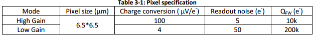
The sensor resolution is up to 150MP (12288 x 12288 pixel). No silicon results yet, but the tapeout was scheduled for May 2014.
The sensor resolution is up to 150MP (12288 x 12288 pixel). No silicon results yet, but the tapeout was scheduled for May 2014.
Rumor: Sony to Announce 22MP Curved Sensor for Mobile Applications
Sony Alpha Rumors quotes Chinese cnBeta site with specs of the first Sony curved image sensor - a 22MP 2/3-inch IMX271SMK and based on it camera module. One of the interesting features of the rumored sensor is rectangular pixels - "Oversampling (2-in-1 Logic physical pixel pixel, without guessing color)":


DPReview quotes another rumor from Chinese website saying that the next generation Sony Xperia Z3X smartphone is to feature the IMX271SMK curved sensor and is scheduled to appear on the market sometime in 2015. The camera phone lens is unusually bright at F1.2.
DPReview quotes another rumor from Chinese website saying that the next generation Sony Xperia Z3X smartphone is to feature the IMX271SMK curved sensor and is scheduled to appear on the market sometime in 2015. The camera phone lens is unusually bright at F1.2.
Sony Invests More in Stacked Sensors Production
Sony plans to invest 35 billion yen in its Nagasaki Technology Center ("Nagasaki TEC") and Kumamoto Technology Center ("Kumamoto TEC") from the H2 of the fiscal year ending March 31, 2015 (FY14) through the H1 of the fiscal year ending March 31, 2016 (FY15), to increase its production capacity for stacked image sensors. The investment is intended to reinforce Nagasaki TEC's "layering process" production capabilities, as well as Kumamoto TEC's "mastering process" facilities. "The layering process refers to the layering semiconductor chips containing back-illuminated structure pixels with semiconductor chips containing the circuit for signal processing. The mastering process refers to the manufacture of photodiodes and wiring processes for stacked CMOS image sensors."
On January 29, 2014, Sony announced its plans to establish and invest in Yamagata TEC as a facility mainly conducting the mastering process. The current investment is expected to enable Sony to complete subsequent stages of production, including the layering process, at Nagasaki TEC on semiconductor chips that have undergone the mastering process at Yamagata TEC, providing Sony with a fully integrated production system for stacked CMOS image sensors. This investment is a part of Sony's mid - to long-term plan to increase its total production capacity for image sensors to approximately 75,000 12-inch wafers per month, and is expected to increase the current capacity of approximately 60,000 wafers per month to approximately 68,000 wafers per month by August 2015.
Over FY14, Sony is going to invest approximately 9 billion yen (Nagasaki TEC: 3 billion, Kumamoto TEC: 6 billion). Approximately 26 billion yen is to be invested in FY15 (Nagasaki TEC).

Thanks to DG for the news.
On January 29, 2014, Sony announced its plans to establish and invest in Yamagata TEC as a facility mainly conducting the mastering process. The current investment is expected to enable Sony to complete subsequent stages of production, including the layering process, at Nagasaki TEC on semiconductor chips that have undergone the mastering process at Yamagata TEC, providing Sony with a fully integrated production system for stacked CMOS image sensors. This investment is a part of Sony's mid - to long-term plan to increase its total production capacity for image sensors to approximately 75,000 12-inch wafers per month, and is expected to increase the current capacity of approximately 60,000 wafers per month to approximately 68,000 wafers per month by August 2015.
Over FY14, Sony is going to invest approximately 9 billion yen (Nagasaki TEC: 3 billion, Kumamoto TEC: 6 billion). Approximately 26 billion yen is to be invested in FY15 (Nagasaki TEC).
 |
| Nagasaki Technology Center (left) and Kumamoto Technology Center (right) |
Thanks to DG for the news.
Mobileye Plans IPO at $3.8B Valuation
Reuters, Globes: Mobileye, a maker of vision & camera-based ADAS systems starts the roadshow for NYSE IPO of $500M at $3.8B valuation. Mobileye's revenue was $81.2M in 2013. Such a high valuation (for a hardware company) reflects the market expectations for a wide adoption of automotive vision systems.
A Youtube video shows one of the Mobileye features in action:
A Youtube video shows one of the Mobileye features in action:
FLIR Announces Availability of its Low Cost Thermal Imager
Marketwired: FLIR announces that the FLIR ONE thermal imaging accessory for smartphones will be available on July 23 for pre-order online at FLIR.com/FLIRONE. The award-winning FLIR ONE transforms an iPhone 5 or 5s into a thermal imager. When paired with its iPhone app, FLIR ONE displays live infrared imagery that allows the user to see the world from a thermal perspective. FLIR ONE will also be available to buy in Apple Stores and on Apple.com in August.
A Youtube commercial explains why average consumer needs thermal camera:
Thanks to SF for the news.
A Youtube commercial explains why average consumer needs thermal camera:
Thanks to SF for the news.
DALSA on CMOS Sensors Today and Tomorrow
Spectronet publishes Teledyne-DALSA presentation "CMOS Today & Tomorrow." Few slides from the presentation:


Subscribe to:
Comments (Atom)
