Day of Small News

Day of Small News

PR Newswire: As has been reported earlier, a settlement between Lead Plaintiffs and OmniVision, Shaw Hong, Anson Chan, and Aurelio "Ray" Cisneros (the "Individual Defendants" and collectively, with OmniVision, the "Defendants") in the amount of $12,500,000 has been proposed by the Settling Parties. A hearing will be held before the United States District Judge on June 5, 2015.

Meanwhile, SeekingAlpha speculates about the chances that Omnivision buyout deal goes through:

"Officers and directors, as a group, own less than 5% of the company, and don't appear to be personally incentivized toward a sale. (CEO Shaw Hong, for instance, would earn profit about $2.7 million off a sale at $30, relative to current prices. His annual compensation has averaged $3.9 million over the last three years.)

In addition, it's not at all clear that such a buyout could get done. The federal government's Committee on Foreign Investment in the U.S. (CFIUS) would likely be involved, and at least one expert sees the combination of foreign ownership and the inclusion of state-owned Shanghai Pudong Science as being a potential roadblock. An agreement now or in the near future could see the approval process run into the 2016 elections, when, as Derek Scissors told Barron's, "the general economic mood is anti-foreign and certainly anti-China."


Micro Market Monitor: The South American image sensor market, mainly driven by the increasing demand for cameras in smartphones and tablets, along with the increasing application of image sensors in the South American medical diagnostic and image sensor market was estimated to be $622.3 million in 2014 and is projected to reach $1,053.6 million by 2019 at a CAGR of 11.1% from 2014 to 2019.
Yole Word on Sony CCD End of Life

Yole Word on Sony CCD End of Life

IMVEurope publishes thoughts by Yole Developpment analyst Pierre Cambou on Sony CCD end of life decision. One quote:

"It is always sad for technologists to watch the creative destruction of technology shifts. I believe this major transition will renew the innovation drive of the industry. Let’s buckle up for a new technology cycle. I am convinced we are not to be disappointed. CCD image sensors are dead, long live CMOS image sensors!"

Synopsys Announces Power-Efficient Vision Processing IP

PR Newswire: Synopsys announces its new DesignWare EV Family of vision processors. The EV52 and EV54 vision processors are fully programmable and configurable vision processor IP cores that deliver over 1000 GOPS/Watt power efficiency, said to be 5X better efficiency than other available vision processors. The cores can operate at up to 1 GHz in a typical 28nm process. The DesignWare EV52 and EV54 Processors are scheduled to be available in May 2015.

Toshiba Starts Mass Production of 1080p 2.7um Pixel HDR Sensor

Business Wire: Toshiba starts mass production of the previously announced 1/3-inch 1080p60 TCM3232PB sensor at the end of April. The PR stated the sensor HDR mode provides 108dB DR, while the flyer talks about 100dB:

Night Vision Eye Drops

Engadget, Business Insider, Newsweek: The same group Science for the Masses that has shown the human vision extension to IR, now publishes another experiment showing night vision improvement with eyedrops. The group used Chlorin e6 cancer treatment substance mixed with insulin for their experiment. They claim that the eyedrops significantly enhance night time vision at distances up to 50 meters for a time of few hours.

The experimenter, Gabriel Licina describes his feelings "It’s subtle. It’s not like ‘oh my gosh I have super vision!’ It’s more like dark became dim, everything was a little brighter. Not a crazy noticeable light, burning and doom, but more a subtle, ‘oh I can see a thing!"

The adverse effects of the proposed solution have not been studied.

SPIE Award for Seek Thermal Camera

SPIE has published a video of its Prizm Award ceremony for Seek Thermal & Raytheon consumer-grade thermal camera, a competitor of FLIR One:


One can see a teardown of Seek Thermal camera and its comparison with FLIR One in mikeselectricstuff videos: Part 1 and Part 2, as well as the analysis of its thermal gradient artifacts.
Point Grey Comments on Sony CCD Line Closure

Point Grey Comments on Sony CCD Line Closure

Point Grey confirms that Sony will discontinue operations of their CCD 200mm wafer line at Kagoshima Technology Center in Japan by the end of March 2017. This line is responsible for production of all Sony CCD image sensors used in Point Grey cameras. Point Grey did not confirm exact last-time buy (LTB) or last-time ship (LTS) dates for the affected CCDs, commenting that recently publicized dates of August 2015 and March 2020, respectively, should not be considered final. “Point Grey has been actively discussing details about the closure directly with Sony,” said Michael Gibbons, Director of Sales and Marketing at Point Grey. “This is a very dynamic situation and final details, including official last-time buy and ship dates, have not yet been released publicly by Sony. We caution our customers against making quick decisions based on preliminary information circulating the Internet.

Point Grey continues to see high and growing demand worldwide for both CCD and CMOS sensor technology, and believes that CCD technology will continue to play an important part in the imaging world for many years to come. “Our goal is to provide customers with three options,” said Gibbons. “First is to continue to buy their existing Sony CCD-based cameras for the natural lifespan of the systems they’re designed into. If customers are happy with these products there is no need to change. For those customers who still prefer CCD technology but want to explore alternatives to Sony, we are actively adding new CCDs from suppliers such as Sharp into our camera lineup. And finally, for those customers interested in the benefits of CMOS technology, we will continue to lead the charge in integrating image sensors from companies like Sony and On Semi into our products.

Xintec to List on Taiwan Stock Market

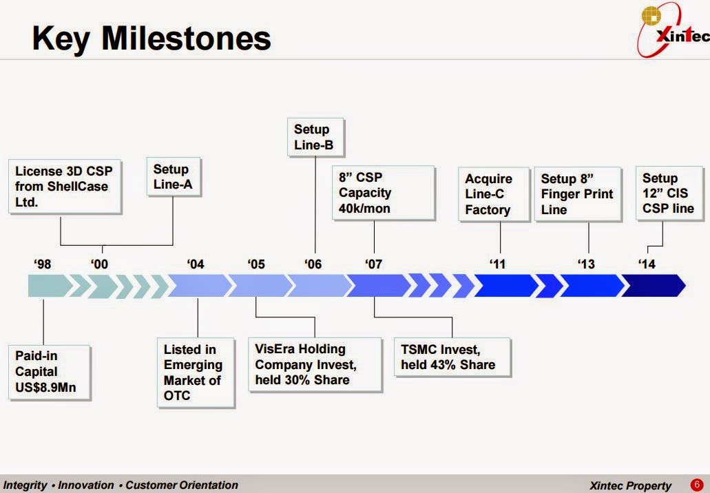
Digitimes: Image sensor wafer-level packaging house Xintec will be listed on the Taiwan over-the-counter (OTC) stock market at the end of March. Xintec is a TSMC and Visera affiliate and reported revenues of NT$4.93 billion (US$158M) for 2014. The company presentation gives some background info:

Ziptronix Stacked Sensor Technology Presentation

Ziptronix kindly sent me its CTO and VP R&D Paul Enquist's presentation at 2015 Image Sensors Conference held last week in London, UK. Few key slides from the presentation:

Forza Selects Silicon Frontline's IR Drop and Resistance Mapping Tool

Forza Selects Silicon Frontline's IR Drop and Resistance Mapping Tool

Marketwired: Silicon Frontline Technology announces that Forza Silicon has selected the company's P2P (IR Drop and Resistance Mapping) for fast, early IR Drop analysis and full-chip verification of their CMOS image sensors.
"Forza Silicon is focused on providing customers with cutting-edge image sensor solutions and we have stringent verification requirements in order to deliver high quality imagers," said Kevin Johnson, CAD Manager at Forza Silicon. "We selected Silicon Frontline's P2P to perform full-chip powernet analysis of our CMOS image sensors designs because it meets our accuracy, speed and quality standards."

Resistance Mapping may be performed at any point in the design cycle, allowing early identification and fixes of problem areas. This ensures detailed IR drop and electromigration analysis is performed with a good candidate design, providing faster time to design closure and earlier market entry.

Tobii Plans IPO

Eye tracking camera and software maker Tobii plans IPO on Nasdaq Stockholm, Sweden. However, this news is forbidden to distribute in the USA, Australia, Canada, Switzerland, South Africa, Singapore, Hong Kong and Japan. Everybody can get more details following the link after the declaration that he's not citizen or resident of the above countries.

The company has been founded in 2001 and now has 600 employees in Sweden, USA, China, Japan, Germany, UK, and Norway. Its 2014 annual turnover is 621M SEK ($73M).

Tobii PCEye Explore entry level eye tracker

Ricoh Pixel Shift Exploits Bayer CFA Properties

Imaging Resource: Ricoh reveals pixel shift technology which utilizes Bayer pattern properties to minimize the interpolation artifacts: "Ricoh's special pixel-shift enhancement mode involves shifting the sensor in one-pixel increments up and down and back and forth, so after four exposures, each pixel contains full RGB data. The end image has the same number of megapixels as the sensor itself, but the data is of much higher quality, with no interpolation needed to "fill in" missing color or luminance information."

Biometrics News

Fujitsu presents smartphone prototype with iris authentication. The active LED and camera system has been exhibited at the MWC 2015 and received the "Best Innovation Award" from AndroidPIT:


Fujitsu Youtube video in Japanese promotes the iris ID system:


In another news, the oncoming Microsoft Windows 10 features Hello component: "Windows Hello will make Windows 10 more personal by providing instant access to your devices through biometric authentication – using your face, iris or fingerprint to unlock your devices – with technology that is significantly safer than traditional passwords. We’re working closely with our hardware partners to deliver Windows Hello-capable devices that will ship with Windows 10. We are thrilled that all OEM systems incorporating the Intel RealSense F200 sensor will fully support Windows Hello, including automatic sign-in to Windows."

"For facial or iris detection, Windows Hello uses a combination of special hardware and software to accurately verify it is you – not a picture of you or someone trying to impersonate you. The cameras use infrared technology to identify your face or iris and can recognize you in a variety of lighting conditions."

The company Youtube video explains its use cases:

Lytro Raises $50M, Restaffs, Retargets

Re/code, LightField Forum: Lytro raised $50M in a round led by a new investor GSV Capital and includes participation from all of Lytro’s existing investors along with Allen & Co. and Danhua Capital. It values the company at five times its last financing round.

Lytro plans to use the new funding to make a strategic shift, taking its light-field technology into new areas, including video and virtual reality.

Lytro CEO Jason Rosenthal told Re/code “Fifty million dollars is a nice big number, but it is not unlimited. We had to make some pretty tough decisions. We are going to have to make some cuts in some areas so we can staff up in some new ones.” The company is expected to lay off 25 to 50 people out of its 130 employees, while at the same time looking to hire those with expertise in the new areas that were not previously of focus for the company.

Late last year, Lytro founder and Chairman Ren Ng announced he was leaving full-time work at the company to take a professorship at the University of California, Berkeley.

Meanwhile, Lightfield Forum reviews a recently published Lytro patent application with movable lightfield lens array to allow the camera operate in both lightfield and a regular 2D imaging mode:

Rambus Oversampled Pixel Patent Application

A 71-page long Rambus patent application US20150070544 "Oversampled image sensor with conditional pixel readout" by Craig Smith, Michael Guidash, Jay Endsley, Thomas Vogelsang, and James Harris expands the previously published applications (1, 2, 3) to 4T-like pixels with added transistor for a conditional reset. There are two versions, both featuring an additional "transfer-enable transistor 253", both able to operate in a partial charge transfer mode:

IP stands for "Image Pixel"
Strategy Analytics: Samsung Has Largest Smartphone CIS Market Share in Units

Strategy Analytics: Samsung Has Largest Smartphone CIS Market Share in Units

Strategy Analytics publishes "Smartphone CMOS Image Sensor Market Share 2014" report. The market for CMOS image sensors in smartphones increased by 28.5% to 2.41 billion units in 2014. The smartphone image sensor market is largely dominated by Sony, Samsung and Omnivision who together accounted for almost 60% of 2014 shipments. Main camera sensors accounted for 55.4% of the total smartphone image sensor market in 2014 with front facing camera sensors accounting for the remaining 44.6% (up from 26.8% in 2010). Samsung is said to have a narrow market share lead, as measured in units.

ULIS Announces Low-Cost VGA Thermal Imager

ULIS announces Pico640 Gen2 low cost VGA/120fps thermal sensor for security and surveillance applications. The 17um microbolometric pixel sensor is aimed to "making thermal imaging more accessible. In addition to security and surveillance systems, ULIS’s new sensor can also be used in cameras for outdoor leisure, such as nature observation or hunting."

The new sensor's NEDT is below 50mK, a more than 15% improvement over ULIS earlier generations, without any trade-off in power consumption. It operates at less than 130mW with a 60Hz frame rate. Other thermal imaging sensors in this category are siid to consume more power, typically 200 to 350mW at an equivalent frame rate. Pico640 Gen2 is housed in ceramic packaging, a cost-saving production technique ULIS first introduced to the market ten years ago. It has shown its value and vacuum integrity in the 500,000 ULIS thermal image sensors already in the field.

Strategy Analytics on Vision-Based ADAS

Strategy Analytics publishes its GPU Technology Conference 2015 presentation "Vision-Based ADAS: Seeing the Way Forward" by Ian Riches. Few interesting statements:


Other ADAS-related presentations at the conference:

Audi driverless car presentation "zFAS the Brain of piloted Driving and Parking" by Matthias Rudolph.
Nvidia presentation "Visualizing a Car's Camera System" by Gernot Ziegler.

Xintec 12-inch WLCSP Line Ready for Mass Production in 2H 2015

Digitimes: Image sensor packaging house Xintec plance to have its 12-inch WLCSP production line ready 2H 2015. Xintec started to invest in its 12-inch WLP-CSP production capability in Q4 2014. TSMC holds an about 40% stake in Xintec. Orders placed by TSMC contribute about 35% to Xintec's overall revenues at present, followed by orders from OmniVision with 29%, according to Digitimes sources.

Sony Expands its Ziptronix Licensing Agreement to Multi-Million Stacked Chip Interconnects

Marketwired: Ziptronix announces a patent licensing agreement with Sony for application in advanced image sensors. The agreement is a continuation of the previous ZiBond agreement extended to Ziptronix's new DBI hybrid bonding patents for high volume applications.

"This license agreement with Sony is an exciting milestone for Ziptronix because it removes any doubt that our patented DBI hybrid bonding technology is both manufacturable and beneficial for high volume applications," noted Dan Donabedian, CEO and president of Ziptronix. "We believe it demonstrates that our patented hybrid bonding technology is both enabling and cost effective as compared to stacking with TSVs. Sony licensed Ziptronix's ZiBond direct bonding patents in 2011, which we also believe grew their image sensor market share from a few percent to the largest market share in the industry. We expect this new license for Ziptronix's DBI hybrid bonding patents will further contribute to Sony's growth within the industry. Any company wishing to compete in this space will need Ziptronix's DBI hybrid bonding patents."

DBI Fact Sheet lists the technology's features:

  • Interconnect pitch ≤10µm
  • Accommodates 1.5M connections/cm2
  • No adhesives, solders, pressure, underfill or wire bonding required to bond and connect layers of active devices
  • Uses standard fab tools and processes
  • Highest reliability of all 3D processes because of hermetic sealing
  • Accommodates face-to-face architectures (top die/wafer upside down)
  • Accommodates face-to-back architectures (use of through-die vias/buried contacts)

Ziptronix DBI page says:

"DBI can achieve over 100,000,000 electrical connections per square centimeter; a significant increase over the ~ 100,000 connections per square centimeter density achieved with through-die vias used in other 3D interconnect approaches."


A Youtube video shows how it works:

Teradyne Enhances 750 Series Testers to Support up to 128MP Image Sensors

Business Wire: Teradyne announced the IP750Ex-HD testers to increase the parallel test capability for both wafer and final test of image sensors using new, High Density (HD) instruments. These instruments are also compatible with over 4,000 installed J750 and IP750 test systems providing added flexibility to test system operators.

New IP750Ex-HD capabilities include:
  • HSD800 Multifunction Instrument. A third generation digital instrument providing 128 high speed digital channels, scalable to 2,048 channels per system.
  • ICMD. A new LVDS image capture instrument supporting MIPI CSI-2 D-PHY 1.5Gbps speed at 1,2,4 Data Lane CIS and Serial 1 to 16 Lane protocol support capability. This second generation instrument has 24 differential input pairs and 128M pixel capture memory .
  • IG-XL 3.60 Software.
  • Zero-footprint, Air-cooled System.
"The IP750Ex-HD uses the same HD instruments as the J750Ex-HD, which has a large installed base and TAM, providing the flexibility in manufacturing to tackle a broad range of SOC and Image Sensor devices. Adding an additional Image Capture Instrument chassis also increases the ICMD slots and allows the IP750Ex-HD to expand to higher site counts," said Jason Zee, General Manager of Teradyne's Consumer Business Unit. Teradyne has received multiple orders from multiple customers and began shipments of the IP750Ex-HD systems in the fourth quarter of 2014.

Sony Stacked Sensor Features Internal Transformer

Chipworks reverse engineers Sony 2nd generation stacked sensor, the 13MP, 1.12um pixel IMX214, first announced about a year ago.

The main features of this stacked BSI device when compared to the respective features on the first generation stacked CIS are:
  1. refinement and modifications to the TSVs used to connect CIS signals to the ISP circuitry
  2. simplification of the manufacturing process to enable lower cost of manufacturing
  3. moving of most of the circuitry from the CIS die to the ISP die, d) changes in pixel circuitry for SME functionality
  4. changes in the organic layer stack on the light receiving side of CIS to bring microlenses closer to the pixel cathodes.

IMX214 bottom (logic) die

But the most intriguing part of the report is a small transformer somewhere on the chip:


If vias can be an indication of the transformer size, its inductance appears to be well below 100pH. Such inductors are not very useful at frequencies below 10GHz. I wonder why does Sony need it?

Update: Chipworks says that transformer part is just a generic marketing image, not related to IMX214 circuitry. The report flyer will be modified soon and the transformer image will be removed.

Another Chipworks report covers 28.2MP Samsung DSLR BSI sensor S5KVB2XX09, featuring 3.6um pixels. The highlights of this report are:
  • Samsung is the first to market with a back-illuminated APS-C format CMOS image sensor
  • An array of partially masked pixel pairs is embedded in the active pixel array to facilitate the phase-detection AF functionality
  • A new shared-pixel architecture is employed for the active pixel array
Dual Aperture Gets More Money from Strategic Partner

Dual Aperture Gets More Money from Strategic Partner

PRNewswire: Dual Aperture International ("DAI") announces a strategic partnership with SK Telecom ("SKT") in a development of DAI's 3D camera technology based on dual aperture 4-color (RGB-IR) sensors. SKT becomes a strategic investor and partner to DAI alongside a $1.4M investment, joining the previously closed $5.7M Series A funding round led by Korean venture capital fund Value Invest Korea.

SKT will develop applications and additional use cases for DAI's 3D image capture, virtual reality and image enhancement technologies. Prof. Chong-Min Kyung, CTO of DAI, commented that, "SKT is a global technology leader with the size and expertise to accelerate DAI's product implementation into global industries spanning mobile, medical, security and automotives. Korea already has a strong technological position in these growing industries, and the partnership between SKT and DAI will only further improve Korea's ability to provide innovative technologies and solutions to these markets."

In Korea, DAI will continue to refine its own technology while SKT will help define new applications for 3D cameras. In the US, DAI and SK Telecom Americas (SKTA) will jointly set up a consumer applications development lab under SKTA's Innopartners program in order to recruit innovators to develop new 3D, virtual reality, image related applications for various markets including Mobile, Medical, Security and Automobile applications.

DAI will also collaborate with Daejeon Creative Economy Innovation Center of the Ministry of Science, ICT and Future Planning, in actively looking for technologies and patents to foster globally competitive start-ups.

Dual Apertures technology is presented in its patent here.

Sony Confirms its Image Sensor Sales Forecast

Sony reports its quarterly results for the quarter ended on Jan 31, 2014. Essentially, the report confirms the company's Feb. 2015 forecast for the image sensor sales:


Sony earnings release says on Devices segment results: "Sales increased 38.6% year-on-year (a 26% increase on a constant currency basis) to 292.9 billion yen (2,421 million U.S. dollars). This significant increase was primarily due to a significant increase in sales of image sensors reflecting higher demand for mobile products, the favorable impact of foreign exchange rates, as well as a significant increase in sales of camera modules. Sales to external customers increased 47.2% year-on-year."

LCC Package Cuts CMOSIS Sensor Price in Half

CMOSIS is to start sampling low-cost versions of its global shutter CMV2000 (2.2MP/340fps) and CMV4000 (4.2MP/180fps) imagers in May 2015. The new versions differentiate from their CMV equivalents by their IC package, being LCC (Leadless Ceramic Carrier) instead of µPGA. The company is to offer the CMV2000/ CMV4000 imagers at about half the price of the current µPGA versions for volumes over 5000 pcs/year. Besides being lower priced, the LCC-type package offers the additional benefit of surface mount assembly, allowing more compact cameras designs and more economical camera assembly.

"We are delighted to explore new and highly attractive market segments for our proven state-of-the-art CMV product line", said Lou Hermans, COO of CMOSIS. "The LCC packaging format will open up a host of high-volume applications and further broaden our strong worldwide position and customer base for advanced camera designs."

CMOSIS sensor in the new package
More Reactions on Sony CCD Decision

More Reactions on Sony CCD Decision

One of the biggest European machine vision camera vendors, Stemmer Imaging, posts a Q&A session with Mark Williamson, its Director of Corporate Market Development, on Sony decision to discontinue CCD products. Generally, Mark agrees that CCD era is over, although "The importance of the CCD to mankind was recognized by a Nobel prize in Physics in 2009. In the last few years there has been a big shift from CCD to CMOS in these high volume markets which has left the CCD wafer line very underutilized even with the high number of machine vision sensors sold. This makes the factory no longer financially viable."

Other quotes:

"In 2010, 22% of cameras we sold were based on CMOS sensors. This has risen to 58% in 2014 with 32% of cameras using Sony CCDs and the remainder other high end CCDs. With nearly all new camera designs using CMOS the prediction is that in a further 4 years the natural shift would make the CMOS market share approximately 80%."

"The higher end CCDs from ON Semiconductor (formerly Truesense and Kodak) and the full frame CCDs used in professional photography from Teledyne DALSA are still available for high end applications although over time CMOS will affect this market segment also."

IMV Europe too publishes an article on the Sony CCD news, mostly quoting machine vision camera vendors reports.

Zoom for Curved Sensors

When Sony curved sensors were presented on summer 2014, there were concerns about their compatibility with zoom lens. Palo Alto, CA-based Optiz proposes a solution. The company believes that curved sensors will be the next big wave in mobile imaging:


Optiz does not say much about the principle of its approach, other than usual marketing words:

"Optiz's proprietary Zoom solution realizes Zoom function in the mobile imaging system without the drawback of conventional solutions."

"Optiz's proprietary pixel architecture technology includes pixel pattern design, photodiode structure and advanced imaging algorithms. With inventive thinking, we have re-imagined these three crucial aspects of the pixel technology and made great advancements in zooming, luminance and color accuracy. All doing so without creating additional complexity to the imaging system while enabling zoom function and reduce module size."

"Our innovative solution offers an optical interface structure that is built into the image sensor chip, thus imaging system need fewer lenses, simplifies the overall optical design and improves image quality."

"Optiz's Zoom solution offers a set of proprietary technology to enable greater sensitivity, lower module profile, superior zooming and dynamic focusing capabilities all without moving parts."

"The innovative pixel architecture provides significant advantages such as reduced cross talk between the pixels at the periphery of the sensor, substantial improvement of Quantum efficiency."

The company has been founded by Vage Oganesian, former Tessera VP R&D, and Wang Wei, CEO of WLCSP. Few pictures from the company site might give some hints on its technology:


Update: I received an email from Optiz saying:

"In regards to the comments on the blog post. We want to clarify that our curved sensor with varying size photodetector does not require physical bending/deformation of the image sensor. We took a conceptually different approach in obtaining the curved structure of image sensor during the fabrication process; So that our image sensor can remain stackable as most of the commercial BSI sensors of today."