Omnivision Samples RGB-Ir Sensor for Biometric Applications

PRNewswire: OmniVision announces the OV2744, a 1.4um PureCel sensor featuring its second-generation RGB-Ir technology which delivers quality IR output without compromising RGB images. The OV2744 targets biometric applications such as facial recognition for front-facing cameras in notebooks, tablets and smartphones.

"Notebook and mobile device OEMs have traditionally relied on two-camera solutions for image capturing and facial recognition functionalities," said Arun Jayaseelan, product marketing manager at OmniVision. "The OV2744 is capable of delivering both premium RGB imaging and high quality IR information required for biometric and other emerging IR applications. The OV2744 thus gives OEMs the opportunity to move to single camera solutions, thereby reducing cost and space requirements for their devices."

The OV2744 is said to have less color aliasing than competing RGB-Ir sensors that are currently available in the market.

The OV2744 captures 1080p video at 60fps while consuming less power than any other 1080p sensor currently on the market. The 1/6-inch OV2744 supports full frame staggered high dynamic range and features an ultra-low power mode, which reduces the resolution and frame rates to conserve additional power.

The OV2744 is currently available for sampling and is expected to enter volume production in Q1 2016.

Qualcomm Low-End AP Supports 16MP Camera

Qualcomm announces its mid-range and low-end SnapDragon mobile processors: 625, 435, and 425. Even the lowest cost 425 model features dual ISP and 16MP imaging support:

ISSCC Review - Part 3

ISSCC Review - Part 3

Albert Theuwissen concludes his ISSCC review with NHK/Shizuoka Univ./Brookman 33MP, 1.1um pixel sensor for 8K UHDTV, and FBK SPAD imager that only reacts when a pre-set number of photons is registered by a pixel.
Image Sensor Conference in Japan

Image Sensor Conference in Japan

Technical Group on Information Sensing Technologies (IST), the Institute of Image Information and Television Engineers (ITE), holds an image sensor conference at NHK Lab facilities, Tokyo, Japan, on March 11, 2016. Participation is free of charge, no prior registration is required. The IST conference proceeding is about 1000-2000 yen. The agenda of the conference is full of interesting presentations:

  • Invited Talk: Low-Noise Image Sensors
    Shoji Kawahito (Shizuoka Univ.)
  • Multi-storied photodiode CMOS image sensor for multiband imaging with 3D technology
    Yoshiaki Takemoto, Kenji Kobayashi, Mitsuhiro Tsukimura, Naohiro Takazawa, Hideki Kato, Shunsuke Suzuki, Jun Aoki, Toru Kondo, Haruhisa Saito, Yuichi Gomi, Seisuke Matsuda, Yoshitaka Tadaki (Olympus)
  • A CMOS Image Sensor Using Multiple Tap Lateral-Electric-Field Charge Modulators for Time-of-Flight Range Imaging
    Taichi Kasugai, Sang-Man Han, Hanh Trang, Taishi Takasawa (Shizuoka Univ.), Satoshi Aoyama (Brookman Tech.), Keita Yasutomi, Keiichiro Kagawa, Shoji Kawahito (Shizuoka Univ.)
  • Stacked Image Sensor Using Chlorine-doped Crystalline Selenium Photoconversion Layer Composed of Size-controlled Polycrystalline Particles
    Shigeyuki Imura, Kazunori Miyakawa, Hiroshi Ohtake, Misao Kubota, Kenji Kikuchi (NHK), Toru Okino, Yutaka Hirose, Yoshihisa Kato (Panasonic), Nobukazu Teranishi (University of Hyogo)
  • A 1280x720 single-photon detecting image sensor with 100dB dynamic range using a sensitivity boosting technique
    Manabu Usuda, Yusuke Sakata, Seiji Yamahira, Shigetaka Kasuga, Mitsuyoshi Mori, Yutaka Hirose, Yoshihisa Kato, Tsuyoshi Tanaka (Panasonic AIS)
  • A 1.1μm 33Mpixel 240fps 3D-Stacked CMOS Image Sensor with 3-Stage Cyclic-Based Analog-to-Digital Converters
    Toshiki Arai, Toshio Yasue, Kazuya Kitamura, Hiroshi Shimamoto (NHK STRL), Tomohiko Kosugi, Sungwook Jun, Satoshi Aoyama (Brookman Technology), Ming-Chieh Hsu, Yuichiro Yamashita (TSMC), Hirofumi Sumi (The University of Tokyo), Shoji Kawahito (Shizuoka University)
  • Visualization of Ultra High-Speed Phenomena by 10 Mfps Ultra High-Speed Camera with Improved Photosensitivity of ISO 16000
    Manabu Suzuki, Masashi Suzuki, Fan Shao, Rihito Kuroda (Tohoku Univ.), Nobuyuki Tokuoka, Yasunori Kawaguchi, Hideki Tominaga (Shimadzu), Shigetoshi Sugawa (Tohoku Univ.)
  • An APS-H size 250Mpixel CMOS Image Sensor Using Column Signal ADCs with Dual Gain Amplifiers
    Takashi Muto, Hirofumi Totsuka, Toshiki Tsuboi, Daisuke Yoshida, Yasushi Matsuno, Masanobu Ohmura, Hidekazu Takahashi, Katsuhito Sakurai, Takeshi Ichikawa, Hiroshi Yuzurihara, Shunsuke Inoue (Canon)
  • A 1.2e- Temporal Noise 3D-Stacked CMOS Image Sensor with Comparator-Based Multiple Sampling PGA
    Kei Shiraishi, Yasuhiro Shinozuka, Tomonori Yamashita, Kazuhide Sugiura, Naoto Watanabe, Ryuta Okamoto, Tatsuji Ashitani, Masanori Furuta, Tetsuro Itakura (Toshiba)
  • An 18M-pixel CMOS Image Sensor Using 12-bit Column-Parallel Single-Slope ADCs with Operation-Period-Reduced Time-to-Digital Converters
    Yoshio Hagihara, Yusaku Koyama, Takanori Tanaka, Atsuko Kume, Yosuke Kusano, Mai Arita, Masashi Saito, Yoshihisa Okada (Olympus)
  • High-Speed Range Finding using Smart Image Sensor
    Daisuke Uehara, Makoto Ikeda (UTokyo)
  • CMOS Biosensor IC Focusing on Dielectric Relaxations of Biological Water with 120GHz and 60GHz Oscillator Arrays
    Takeshi Mitsunaka, Akira Saito, Nobuyuki Ashida, Kunihiko Iizuka (SHARP), Tetsuhito Suzuki, Yuichi Ogawa (Kyoto Univ.), Minoru Fujishima (Hiroshima Univ.)
  • Device Simulations for Ultrahigh-Speed and High-Voltage Image Sensors
    Hideki Mutoh (Link Research)
  • Color Image Sensor with Three-stacked Organic Photoconductive Films
    Toshikatsu Sakai, Hokuto Seo, Tomomi Takagi, Misao Kubota, Hiroshi Ohtake (NHK), Mamoru Furuta (Kochi Univ. of Tech.)
  • Organic-Photoconductive-Film CMOS Image Sensor -- 120dB Wide-Dynamic-Range,Photoelectric conversion controlled Global Shutter --
    Masashi Murakami, Kazuko Nishimura, Sanshirou Shishido, Masayuki Takase, Yasuo Miyake, Tokuhiko Tamaki, Yoshihiro Sato, Yasunori Inoue (Panasonic)

Thanks to RK for the info!
EVG Joins European Wafer Stacking Program

EVG Joins European Wafer Stacking Program

EV Group (EVG) joins the 3D integration consortium of IRT Nanoelec headed by CEA-Leti and includes STMicro and Mentor Graphics to develop advanced 3D wafer-to-wafer bonding technologies. SET also joined recently the consortium.

Séverine Chéramy, director of the 3D integration program of IRT Nanoelec, said the consortium expects to achieve an interconnection pitch of about 1µm.

"Wafer-to-wafer stacking using direct Cu-to-Cu bonding is key for advanced 3D technologies, specifically for imaging application and 3D partitioning," Chéramy said. "EVG's knowledge on bonding will leverage the process expertise of the original members. The participation of EVG in the consortium will create new opportunities and optimized and cost-effective solutions for 3D IC devices."
Himax Updates on its CIS Business

Himax Updates on its CIS Business

Himax reports its Q4 and full fiscal 2015 year results. There are few updates on the company's image sensor business:

"CMOS image sensor business was the main factor behind the year-over year decline. As mentioned in our previous earnings call, our CMOS Image sensor business suffered becaucse we didn’t ramp our 8MP and 13MP sensors as planned due to the lack of Phase Detection Auto Focus (PDAF), a new but nowadays required feature for high end smartphone. We remained one of the market share leaders in notebook sector.

In terms of our 8MP and 13MP CMOS image sensors with PDAF feature, we are catching up fast. We believe we will be one of the few players capable of providing PDAF-equipped CMOS image sensors in the very near future. We will report progress in due course.
"

Panasonic 123dB WDR Organic Sensor

BusinessWire: Panasonic develops a new WDR technology which can improve simultaneous-capture DR 100 times wider than the conventional results, using a CMOS image sensor with an organic photoconductive film (OPF). The Dual-Sensitivity WDR Pixel Technology has two sensitivity detection cells in each pixel, taking advantage of a high-saturation performance and flexibility of a sensitivity setting of OPF CMOS image sensor, in order to achieve simultaneous-capture 123dB WDR. Capacitive-Coupled Noise Canceller Technology cancels pixel reset noise, in order to improve SNR of dark objects.

Panasonic holds 58 Japanese patents and 44 overseas patents (including pending) related to this technology.


Update: Nikkei publishes a 3-page article on this sensor.

Panasonic 10x Higher Saturation Global Shutter Organic Sensor

Businessire: Panasonic develops a new global shutter CMOS sensor using organic photoconductive film (OPF). The technology is said to enable capturing high speed moving object up to 10 times brighter scene in global shutter mode. In OPF CMOS image sensor, charge-storage function and photoelectric-conversion function can be set independently. Motion direction can be detected from acquired object's signal level in one picture by fine control of shutter sensitivity by changing applied voltage to OPF which is hardly realized by conventional CMOS image sensors.

The new technology has the following advantages:

1. Wide incident angle (60 degrees), high sensitivity, high saturation and highly-functional circuits due to a unique feature of OPF, in which an OPF for photoelectric-conversion and a readout circuits are independent.
2. High saturation signal up to 10 times larger than conventional image sensors with global shutter function due to Photoelectric Conversion Controlled Global Shutter Technology.

This development is based on the following new technologies:

1. CMOS Image Sensor Design Technology, in that, an OPF photoelectric-conversion part and a circuit part can be designed independently.
2. Photoelectric Conversion Controlled Global Shutter Technology that is realized by controlling of organic photoconductive film sensitivity.
3. Variable Sensitivity Multiple Exposure Technology which can detect the motion and its direction by changing image capturing sensitivity in each frame.

Panasonic holds 60 Japanese patents and 41 overseas patents (including pending) related to this technology.

Panasonic presented a part of the research at 2016 ISSCC.

Panasonic APD-CMOS Sensor Sees Colors under 0.01 lux Illumination

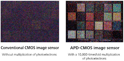
BusinessWire: Panasonic developed APD CMOS sensor with avalanche photodiodes (APDs) in each pixel. The in-pixel APDs multiply the photoelectrons by 10,000 times. This is said to allow getting sharp color images even under starlight (illuminance of 0.01 lux) or in other similarly dark places. Variable sensitivity technology in which multiplication is controlled in a thousandth of a second by controlling the voltage applied to the APDs, realizing 30-fps video imaging that can follow the changes in illuminance.

The new sensor has been presented on the 2016 ISSCC on February 1, 2016.

This development brings the following advantages:
  • Highly sensitive color imaging:
    40 million/lux・sec・μm2 (10,000 times sensitive in comparison to conventional devices)
  • Wide dynamic range:
    100 dB (+ 40 dB in comparison to conventional CMOS image sensors)

Pixart Reports 2015 Results

Pixart reports that its Q4 2015 revenue increased by 1.2% QoQ to NT$1,078.7 million. Due to unfavorable change in product mix, the gross margin decreased from 51.2% in previous quarter to 50.5% in 2015Q4. The revenue for 2015 was NT$4,320.2 million, decreased by 9.0% YoY.

Panasonic Develops 100x More Sensitive Image Sensor

Nikkei: Panasonic developed an image sensor 100 times more sensitive to light than an existing technology. The new sensing layer is made from an organic material film rather than silicon. Panasonic developed the basic technology with Fujifilm. A proprietary readout circuit reduces noise, while a modified electrode structure helps detect even faint light efficiently.

The company says the new sensor does not suffer from blooming, and is aimed to automotive applications.

Blooming demo, Panasonic sensor is on the right.

Possibly, the article material is based Panasonic presentation at ISSCC 2016. The company aims to have a practical version ready as early as 2020 or so.

3D Camera Market Report

PRNewswire: Allied Market Research publishes "World 3D Camera Market - Opportunities and Forecasts, 2014 - 2021" report.

"The global 3D camera market would garner revenue of $10.8 billion by 2021, registering a CAGR of 40.0% during 2016 - 2021. Professional 3D cameras would lead the market throughout the analysis period. The 3D cameras embedded in smartphones are expected to drive the 3D camera market significantly by 2021.

The 3D camera market is in its nascent stage; in 2015, it contributed to about 2-3% of the overall 3D technology market. However, its contribution to global markets, would increase significantly within the forthcoming decade. The market for 3D cameras is primarily driven by the requirement to record 3D content in media & entertainment applications. Other factors, driving the market growth include enhancement of 3D scanning technology, improved user preferences, increasing adoption of home automation applications and enhancement in virtual reality products.

Stereo vision is the largest revenue-generating technology segment of 3D camera market, which accounted for nearly 60% of the total market revenue in 2015. This segment is expected to maintain its dominance throughout the analysis period owing to its cost effectiveness and simplicity in implementation as compared to other technologies. However, time of flight technology is expected to grow at the highest CAGR of 44.6%, during the forecast period.

Among the key applications, professional 3D camera was the largest contributor, which accounted for around 65% share in 2015. However, the tablet applications would exhibit the highest CAGR of over the forecast period, owing to rising adoption of tablets as portable computing solutions.
"

ESPROS Talks about ToF Imaging Challenges

ESPROS Photonics' mailed me the Jan. 2016 Newsletter updating on the company's ToF business success and technical challenges:

"The ESPROS TOF technology is gaining huge momentum. The delivery start of the 3D-TOF QVGA imager was excellent. Customers immediately recognized the performance of our OHC15L technology. A QE of more than 80% at 850nm wavelength and pixels with 100% fill factor provide unmatched sensitivity with very low illumination power. A reference design of a camera engine with a horizontal FOV of 94° achieves a 10m range in the full field. Ok, this is on a white target. But the exposure time is a few milliseconds only."

Then, the newsletter shares the company experience dealing with temperature drift challenges:

"Several components of a TOF system are temperature sensitive: On the 3D TOF chip e.g. pixel-field, LED driver and the phase detector (DLL), etc.; on camera level e.g. the illumination (e.g. LEDs, VCSELs), illumination driver, connectors, IR filters, lenses, etc. Figure 1 shows the signal path with the contributors to temperature drift.


The main contribution comes from the pixel-field which is approx. 85% of the total distance drift by temperature (Figure 2).


The temperature drift in the pixel field is related on the one hand to the drift speed of electrons in solid which changes by temperature. It is a physical constant so it can be compensated by simple temperature measurement of the chip temperature. On the second hand, the drift speed is also related to the field strength in the photodetector. This field is
generated by the the backside voltage VBS. A simple rule says the higher the voltage the faster the electrons (Figure 3). However, there is a voltage limit where other effects start to become dominant. It is to note that a variation of VBS varies the measured distance. Thus, an accurate and constant VBS voltage is mandatory for accurate measurement.


Figure 4 shows a 2nd order fit for the compensation of the temperature drift in the pixel field."

Thesis on Time-Resolved CMOS Sensors with Draining-Only Modulation Pixels

Shuzuoka University publishes an 2013 PhD thesis "A Study on Time-Resolved CMOS Image Sensors with Draining-Only Modulation Pixels for Fluorescence Lifetime Imaging Microscopy" by Zhuo Li. The pixel concept is shown below:

Concept of two-stage charge transfer pixel and draining only
modulation (DOM) pixel.
DOM pixel layout
Photo charge modulation and sequential readout in the
DOM pixel

Pixium Vision Reports Retinal Implant Business Success

BusinessWire: Pixium Vision says it is the only company in the world to develop in parallel two distinct retinal bionic implant platforms. IRIS II, the company’s first system, targeting retinitis pigmentosa, and PRIMA, the second generation miniaturized wireless implant, better suited for Age Related Macular Degeneration (AMD) will allow the company to address an estimated market of more than 4 million patients in Europe and North America.

Over the last quarter of 2015, the company made significant progress on IRIS II, its epi-retinal bionic system equipped with an asynchronous bioinspired image sensor. IRIS II is said to be the first epi-retinal device to be equipped with 150 electrodes worldwide. In December 2015, the company received the approval from the French regulatory authority ANSM to initiate clinical study for patients who have lost sight due to retinitis pigmentosa. The company has also received the Austrian approval. Further national approvals are expected in the coming months.

In early 2016, the company announced positive preclinical safety and feasibility data for PRIMA, its second generation bionic system. Stanford University, demonstrated thermal safety of near infrared stimulation of PRIMA in a well-established animal model for retinal damage assessment in laser treatment.

A Vimeo video explains the company's technology"


Pixium IRIS implant
Pixium PRIMA implant