CISTERN and EXIST Programs Support Image Sensor R&D in Europe

CISTERN and EXIST Programs Support Image Sensor R&D in Europe

Adimec announces its participation in two European projects for advancing CMOS image sensor technology: CISTERN and EXIST. Both programs begin in April/May 2015 and will be completed in 2018.

The main objective of CISTERN, which is an acronym for CMOS Image Sensor Technologies’ Readiness for Next generation of applications. The other partners in this project are Grass Valley (project leader), Thales Angenieux, SoftKinetic, Delft University of Technology, University of Burgundy. CISTERN is a part of CATRENE Program and is aimed to:
  • To develop CMOS imager sensors with improved performance on spatial resolution, temporal resolution, higher bit depths, lower noise, wider color gamut, higher quantum efficiency (not necessarily all combined for each sensor) and additional, smart functionality in the pixels. The consortium will develop imager sensors in the categories UHDTV, Time-of-Flight and hyper- and multi-spectral, for the application areas broadcast, entertainment, and security.
  • To develop real time image processing techniques needed to improve the quality of the digital output signal of the sensor demonstrators.
  • To develop and demonstrate the capability to produce multispectral imagers by hybridization of multispectral filter arrays on top of CMOS sensor.
  • To demonstrate the improved performance of the CMOS imagers combined with related processing in a number of demonstrators.
  • To develop Ultra High resolution, widely opened, sensor adapted zoom lenses (2/3’’ format, 4K resolution) for broadcast and security applications/markets.
  • To optimize lens design in term of performance/cost/weight/camera integration for integral imaging chains.
  • To develop and demonstrate an integrated Camera Lens Assembly for security applications that offers UHDTV performance with Size and Weight of an HDTV solution.
  • To start in-house CMOS image sensor development in Grass Valley.
The EXIST (EXtended Imaging Sensor Technologies) consortium will investigate and develop innovative new technologies for image sensors. The EXIST team consists of R&D institutes advanced in image sensor technologies, image sensor designs and video processing (IMEC, Fraunhofer IMS, Le2i, TNO, iMinds and TU Delft) and fabless design houses, semiconductor manufacturer (Sofradir) and system integrators (CMOSIS, Grass Valley, Softkinetic, Thales Angenieux, Adimec, Silios, Sofradir, Focal, and Quest). The objectives of this program are investigate and develop innovative new technologies for image sensors needed in the next plus one (N+2) generation of several application domains. The image sensor research will focus on enhancing and extending the capabilities of current CMOS imaging devices:
  • New design (architectures) and process technology (e.g. 3D stacking) for better pixels (lower noise, higher dynamic range, higher quantum efficiency, new functionality in the pixel) and more pixels at higher speed (higher spatial and temporal resolutions, higher bit depth), time-of-flight pixels, local (on-chip) processing
  • Extended sensitivity and functionality of the pixels: extension into infrared, filters for hyperspectral and multispectral imaging, better colour filters for a wider colour gamut, and FabryPérot Interference cells
  • Increasing the optical, analog and data imaging pipelines to enable high frame rates, better memory management, etc.
After developing the related technologies, six prototype image sensors will be designed:
  • two high resolution, high frame rate image sensors with 32Mpixels or more;
  • two Time of Flight image sensors;
  • one 3D stacked image sensor.
  • one integrated high performance hyperspectral image sensor
Next to these image sensor designs, the team will make a number of filter designs for integration on top of above mentioned and commercially available image sensors:
  • Multispectral filters for MWIR
  • Hyperspectral filters for NIR-passband and NIR-cutoff filters;
  • HSI filters and BSI imager for VISNIR range;

CogniVue Announces Next Generation Cognition Processor

PRNewswire: CogniVue, which has licensed its APEX Image Cognition Processor (ICP) technology to Freescale, announced that its new APEX Processing Core - Opus - is at the center of the intense battle for ADAS market share as challengers to Mobileye, the current market share leader, line up to capture business for next-generation ADAS systems. Opus is said to have 10x performance increase over the current G2-APEX.

"CogniVue has been anticipating this ADAS market showdown and we are ready to equip competitors to Mobileye with the performance and cost advantages they need to capture new ADAS opportunities," said Simon Morris, CEO of CogniVue. "We have the innovation, technology and engagement with dominant players in the automotive market and key SoC suppliers to be a key enabler of next-generation ADAS and autonomous driving."

ST Explores Its Options with Imaging Business

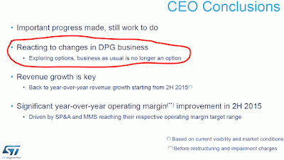
ST has held a 2015 Analyst Day today. The company says it's exploring options to cut losses at its Digital Product Group (DPG), a division that makes image sensors among other products. "This problem needs to be fixed and we will fix it," says CEO Carlo Bozotti (SeekingAlpha).

Meanwhile, DPG presentation says that ST imaging business is focusing on specialized image sensors and proximity sensors, while winding down commodity imaging products:


In spite of the option explorations, the manufacturing presentation talks about imaging and the 3D roadmap:

MDT Announces Magnetic Imagers

PR Newswire: ZHANGJIAGANG, Jiangsu, China-based MultiDimension Technology (MDT), a supplier of Tunneling Magnetoresistance (TMR) sensors, announces the MIS63xx TMR magnetic image sensors. They are said to be the world’s first TMR magnetic sensors for magnetic image scanning with high-resolution in 50DPI. They are designed for financial anti-counterfeit appliances in banknote sorters, ATM, and vending machines. They are also ideally suited for high-resolution magnetic image scanning in non-destructive testing applications.

MDT supplies TMR magnetic sensor wafers or bare dice.

Sony to Increase Image Sensor Capex 4.8x in FY2015

Sony annual report for its FY2014, ended on March 31, 2015, states that its image sensor capex will reach 210 billion Yen in FY2015, about 4.8 times higher than in FY2014:


The same data is included in its updated Semiconductor business flyer, dated by April 30, 2015:

Anitoa Demos DNA Sensing with its Low-Light Fluorescent Imager

PRWeb: Anitoa Systems, a Palo Alto startup established in 2011, partnering with Zhejiang University of China, has demonstrated a handheld real time quantitative-polymerase-chain-reaction system (qPCR) using Anitoa's ultra-low-light CMOS bio-optical sensor. Anitoa’s ULS24 ultra-low light CMOS bio-optical sensor is said to be the first commercially available CMOS sensor that has the needed sensitivity to replace photon multiplier tubes and cooled-CCDs in a wide range of medical and scientific instruments. The ultra-low light sensitivity (3e-6 lux) of Anitoa’s CMOS sensor is crucial for achieving good SNR in imaging molecular interactions based on fluorescent or chemiluminescence signaling principle. “We are very pleased to see the test results coming back from partner hospital showing the effectiveness of detecting infectious pathogens. This not only validates the CMOS bio-optical sensor’s ultra-low-light sensitivity, but also its applicability to real world disease diagnostics”, said Anitoa CEO Zhimin Ding.

ULS24 is built on 0.18um CMOS process at "a world-leader specialty semiconductor foundry."

Anitoa’s Intelligent Dark-current Management architecture. It starts with high responsivity photodiodes.
The readout circuit performs multimodal sensing to capture signal and noise information, the A/D and digital signal processor is said to take advantage of the multi-modal information to achieve better noise cancellation.
IISW 2015 Program: All-Pixel PDAF, Global Shutter Stacked Sensors, and More

IISW 2015 Program: All-Pixel PDAF, Global Shutter Stacked Sensors, and More

2015 International Image Sensor Workshop (IISW) to be held on June 8-11, 2015 in Vaals, The Netherlands, publishes its program. There is quite a lot of interesting papers. Just to name a few of the broader public interest:

Sony and Canon present image sensor with phase detection autofocus in ALL pixels:

A Low Noise and High Sensitivity Image Sensor with Imaging and Phase-Difference Detection AF in All Pixels
M.Kobayashi, M.Johnson, Y.Wada, H.Tsuboi, J.Iwata, T.Ono, H.Takada, K.Togo, Y.Arishima, T.Kishi, A.Okita, H.Takahashi, T.Ichikawa
Canon Inc., Japan

A 4M pixel full-PDAF CMOS image sensor with 1.58μm 2X1 On-Chip Micro-Split-Lens technology
Sozo Yokogawa, Isao Hirota, Isao Ohdaira, Masao Matsumura, Atsushi Morimitsu, Hiroaki Takahashi, Toshio Yamazaki, Hideki Oyaizu, Yalcin Incesu, Muhammad Atif, Yoshikazu Nitta
Sony Japan and Germany

Omnivision, Sony and Olympus present the updates on their latest stacked sensor work:

Stack Chip Technology: A New Direction for CMOS Imagers
V.C. Venezia, H. Rhodes, C. Shih, W.Z. Yang, and B. Zhang
OmniVision, USA

A 3D stacked CMOS image sensor with 16Mpixel global-shutter mode using 4 million interconnections
Toru Kondo, Yoshiaki Takemoto, Kenji Kobayashi, Mitsuhiro Tsukimura, Naohiro Takazawa, Hideki Kato, Shunsuke Suzuki, Jun Aoki, Haruhisa Saito, Yuichi Gomi, Seisuke Matsuda and Yoshitaka Tadaki
Olympus Corp., Japan

A 1/1.7-inch 20Mpixel Back-illuminated Stacked CMOS Image Sensor with parallel multiple sampling
Hayato Wakabayashi, Atsushi Suzuki, Nobutaka Shimamura, Toshiki Kainuma, Kensuke Koiso, Atsushi Masagaki, Yoichi Yagasaki, Shigeru Gonoi, Masatoshi Mizuno, Tatsuya Sugioka, Takafumi Morikawa, Yoshiaki Inada
Sony, Japan

Qualcomm and TSMC present new CFA ideas:

New Color Filter Patterns and Demosaic for Sub-micron Pixel Arrays
Biay-Cheng Hseih, Hasib Siddiqui, Todor Gerogiev, Kalin Atanassov, Sergio Goma, and
HY Cheng, JJ Sze, HY Chou, Calvin Chao, SG Wuu
Qualcomm Inc., USA
TSMC, Taiwan

Basler Vision Campus

Basler publishes a number of image sensors and camera tutorials under the name of "Vision Campus." One of them talks about CMOS sensors superiority over CCDs:

Invisage Updates its Web Site

Invisage launches an updated web site featuring a new Technology page:

Invisage sensor cross-section. Note, there is no microlens.

The technology page also introduces Dynamic Zoom feature - a sort of binning in continuous photoconductive film. Nice idea. I hope they find a way to combine it with CFA:

Interview with Aphesa Founder

Interview with Aphesa Founder

Vision Systems Design publishes an interview with Arnaud Darmont, the founder of Aphesa, on the industrial and machine vision market trends. Few quotes:

Q: In which areas or applications do you see the most growth?

A: There are more and more requests for very high-resolution cameras, although most of customers still require low resolution cameras in the range of 1 to 5 MPixels.

Q: Is there a particular trend or product in the next few years that you see as “the next big thing?”

A: If I knew what the next big thing would be then I would invest in it today. We have seen several recent significant breakthroughs in 3D imaging and in HDR imaging, but who knows what will be coming next.
Harvest Imaging Forum Speaker Announced

Harvest Imaging Forum Speaker Announced

Albert Theuwissen, the host of Harvest Imaging Forum "3D Imaging with Time-of-Flight: Solid-State Devices, Circuits and Architectures" to be held in Dec. 2015, in Voorburg (the Hague), the Netherlands, announces the speaker's name on the forum: David Stoppa, FBK, Italy. Recently, David has worked on SPAD-based imagers for ToF and other applications, while his earlier works cover other image sensing technologies.
Sony Image Sensor Demand Said to Exceed Supply

Sony Image Sensor Demand Said to Exceed Supply

GSM Dome quotes Chinese market analysts saying that a lot of Sony image sensor production capacity has been allocated for Apple iPhone 6c, supposed to be launched in September. Due to that, smartphone companies in China are unable to get enough Sony image sensors for their products. Huawei is said to manage to ship just 50% of its devices with Sony sensors, while ZTE, Oppo and Coolpad are able to get just 10-30% smartphones on the market with a Sony camera module.

As a result, these companies are forced to go to Samsung, Toshiba or Omnivision to complement their supply of image sensors. It is speculated that HTC has chosen Toshiba sensors for its HTC One M8 for that reason as well.

Update: Digitimes sources in Taiwan generally confirm the story. Sony gives priority supply to Apple and Samsung. Supplies of Sony's CMOS image sensors are at least 30% short of demand for China's smartphone vendors including Xiaomi, Huawei, Coolpad and ZTE, according to the newspaper's sources. For some second- and third-tier vendors, the shortage is as high as 70-80% due to a lack of purchasing bargain power.

OmniVision Launches 1/3-Inch Sensor with RGB-IR Color Filter

PRNewswire: OmniVision announces the OV9752, a CameraChip sensor for security and home monitoring applications.

"The OV9752 uses an RGB-IR dual band color filter instead of the traditional mechanical rotary filter, which both simplifies the design and reduces the sensor footprint. This approach also allows the sensor to capture extremely high quality IR images and video, even from great distances," said Chris Yiu, senior strategic marketing manager at OmniVision. "Traditional security cameras' mechanical IR filters are major cause for security camera failures. By eliminating the need for such a mechanical filter, the OV9752 provides our customers with a more reliable and highly effective camera solution."

Built on the 3.75um OmniPixel3-HS pixel, the OV9752 can capture in 1280 x 960 video at 60fps with 10-bit output, or at 45fps with 12-bit output. In addition to a regular operating mode with 165mW power consumption, the OV9752 features an ultra-low power mode, which allows the sensor to reduce the resolution and frame rates and operate at reduced power.

The OV9752 fits into a 6.3 x 5.2 mm package. It is currently available for sampling and is expected to enter volume production in Q4 2015.

Optical Advantages of Curved Image Sensor

This old paper becomes more interesting in light of the recent curved sensor developments. In March 2008, Optics Express published a paper "The optical advantages of curved focal plane arrays" by Staford University team of Seung-Bum Rim, Peter Catrysse, Rostam Dinyari, Kevin Huang, and Peter Peumans:

"...we have shown that a curved imager provides a large degree of freedom in the design of the camera system, helps reduce fundamental aberrations and provides better resolution and brightness. This was demonstrated using designs for a simple and compact camera system by a full analysis of the characteristics of digital imaging systems with planar and curved FPAs."

ON Semi Reports Q1 2015 Earnings

ON Semicondusctor reports Q1 2015 results:

"Now let me provide you an update on performance of our business units, starting with Image Sensor Group or ISG. Revenue for our Image Sensor Group was approximately $171 million, as compared to approximately $166 million in the fourth quarter. Aptina was nicely accretive to our non-GAAP EPS and we remain on track to generate $0.08 of non-GAAP EPS accretion from Aptina in the current year.

...our momentum in fast growing Advanced Driver Assist System (ADAS) market remains intact and we continue to be market leader with approximately 70 percent share for image sensors for ADAS related applications.

...We continue to gain increasing traction with our image sensors in the automotive market. We have high penetration with our image sensors in the Rear View Camera (RVC) market at the OEM level in North America, Japan and Korea. For advanced driver assist systems (ADAS) our 1 megapixel image sensors continued to ramp in Europe and North America. We benefited from strong sales of light trucks in North America as we have higher content in light trucks.

...Robust growth in the security market generated strong demand for our image sensing solutions during the quarter. Specifically, we had strong traction of our 1/3-inch, 720p sensor at leading security OEMs in China. Furthermore, China is beginning a large transition to 1080p security cameras, which will utilize our 2 megapixel, 1/3” and 3 megapixel, 1/3” sensors. We are seeing good penetration globally in the top tier machine vision camera manufacturers for the Python 1.3 megapixel, 5 megapixel, and 25 megapixel devices.
"

ON Semi Revenue Split
Teradyne Reports Higher Image Sensor Tester Sales

Teradyne Reports Higher Image Sensor Tester Sales

BusinessWire: In its quarterly earnings report, Teradyne states "In System-on-a-Chip test, orders grew 66% based on a combination of the success of our new IP750Ex-HD system for image sensor test, continued strength in mobile processors, and growing demand in analog test." The company says that the IP-750 imager test orders are highest in over three years.
Sony Europe Image Sensing Solutions' Statement on CCD Cameras Discontinuation

Sony Europe Image Sensing Solutions' Statement on CCD Cameras Discontinuation

Sony Europe’s Image Sensing Solutions Division, responsible for machine vision, security and industrial cameras under Sony brand, come up with an official statement on its CCD cameras fate:

Sony ISS Senior Marketing Manager, Matt Swinney, said: “Sony CCD-based industrial cameras will not be discontinued due to CCD sensor availability until 2026. There is no requirement to ask our customers to provide ‘last time buy’ estimations because it is not necessary. This is the difference Sony as a complete camera manufacturer brings to the market.

Mr. Swinney added: “2015 is set to be an exciting year for Sony Image Sensing Solutions. New technologies and new product line ups will affect dramatic changes throughout the security, low vision and machine vision industries.

Via Vision Systems Design.