Omnivision Agrees to Be Acquired for $1.9b

Omnivision Agrees to Be Acquired for $1.9b

Reuters, Bloomberg: OmniVision announces that it agrees to be acquired by a consortium composed of Hua Capital Management, CITIC Capital, and GoldStone Investment (collectively, the “Consortium”). Under the terms of the agreement,
OmniVision stockholders will receive a total of approximately $1.9 billion. The agreement was unanimously approved by OmniVision’s Board of Directors.

We are pleased to have reached this agreement, which we believe realizes significant value for our stockholders and offers new opportunities for our employees to develop more innovative solutions for customers.” said Shaw Hong, chairman and CEO of OmniVision. “Our Board unanimously concluded that partnering with Hua Capital Management, CITIC Capital and GoldStone Investment was the best choice for OmniVision, as this transaction will provide our stockholders with significant and immediate cash value. Further, Hua Capital Management, CITIC Capital and GoldStone Investment are highly regarded China-based private equity firms with deep experience in the semiconductor industry. With our new partners’ knowledge and insight and the added flexibility that we will have as a private company, OmniVision will be able to focus on reaching the next level of growth, which will benefit our employees, customers and business partners.

We are excited to partner with OmniVision as they embark on this next phase of growth,” said Yue Liu, a managing director at Hua Capital Management. “We believe our unique industry knowledge and operational expertise can help accelerate OmniVision’s presence both in China and globally.

We are very pleased to be making this investment and are excited about the opportunity to work with OmniVision’s outstanding management team. With the strong backing of the consortium and the leadership of the company’s management, we believe OmniVision will continue to be well-positioned to achieve significant growth through its innovative and superior digital imaging technologies and its commitment to building long-term success,” said Yichen Zhang, Chairman and CEO of CITIC Capital.

OmniVision CEO Shaw Hong is expected to remain with OmniVision in the same capacity. The transaction, which is expected to close in the third or fourth fiscal quarter of fiscal year 2016, is subject to approval by OmniVision stockholders, regulatory approvals, including antitrust review in the U.S. and China, review and clearance by the Committee on Foreign Investment in the U.S., clearance or approval under applicable Taiwan law, and other customary closing conditions. In order to obtain clearance or approval under applicable Taiwan law, OmniVision will divest certain of its investments in Taiwan, including certain of its interests in a joint venture.

Update: As usual in public company acquisition cases, a number of law firms start investigations on grounds that the acquisition price is too low and not in shareholders interests. See the PRs of Tripp Levy PLLC, Bronstein, Gewirtz & Grossman LLC, Wolf Popper LLP, Kahn Swick & Foti LLC, Robbins Arroyo LLP, Harwood Feffer LLP, and, probably, some more.

Microsoft Hololens Cameras

Yesterday's Microsoft presentation of the Hololens AR glasses has shown a complex camera system inside. Each Hololens contains at least 6 different cameras, as far as I can count. If Hololens becomes a mass market device, it could be the single biggest market for image sensors:


A company Youtube video presents the Hololens internal design:


Update: MSDN publishes a video interview with Alex Kipman talking about the Hololens design challenges.

Light Reveals More Details

Light startup officially announces that it has entered into a strategic relationship with Foxconn's FIH Mobile Ltd. As part of the strategic partnership, FIH Mobile Ltd. has licensed the Light technology and made an equity investment in Light.

Calvin Chih, CEO of FIH Mobile, says "We see tremendous potential for Light’s technology, and are excited to work with Dave and the Light team. We continue to strive to help consumers and OEM partners enhance their experiences and product offerings pertaining to high quality imaging."

Paul Jacobs, Executive Chairman of Qualcomm and Light investor and board member says "Light’s product will overcome the current limits of capturing high-quality images in small form factors and will enable people to capture great images while they are on the go without trading image quality for convenience."

ExtremeTech publishes more details on Light technology:

"Light is planning to use an array of small cameras — very similar to those you would find in a smartphone today — to mimic a larger camera. By precisely aligning and calibrating the individual cameras, the images from them can be combined to produce a single image of very high quality. By having some of the cameras feature a wide-angle lens, and some a telephoto lens, an optical zoom capability is also possible.

Light’s CTO, Rajiv Laroia, explains that by treating the ten or more small sensors as pieces of a single, large sensor, Light’s camera module can add together all the photons that reach a particular location in each of the sensors to mimic larger photosites. By adding the signals, the ratio of signal to noise is greatly increased.

Light has also come up with a very clever way to mimic zoom capability using an array of fixed-focal-length (prime) lenses. Its arrays feature both wide-angle and telephoto lenses (it’s planning to have 35mm and 70mm lenses in its first smartphone-sized module) in an overlapping configuration. The telephoto lenses are mounted sideways in the module, to keep thickness to a minimum and allow for a small mirror that can be used to aim the telephoto lenses at different portions of the wide-angle view.
"


Light uses overlapping fields of view to emulate
a single-lens optical zoom. Mirrors move the multiple
70mm lenses to create an overlapping field of view to
provide effective focal lengths between 35mm and 70mm.
The 35mm lenses provide a wide field of view image to
assist in aligning the telephoto images.

Update: As written in comments, Imaging Resource publishes an interview with Light founder, their background and their projections into the future of mobile photography.

Image Sensor Market Shares

WSJ article "How Sony Makes Money Off Apple’s iPhone" shows TSR 2014 pie chart on image sensor market shares:


WSJ writes:

“Unlike memory chips, making image sensors requires craftsmanship, and that’s not something competitors can copy in the short term,” says Hideaki Miwa, analyst at Techno Systems Research Co.

According to the Tokyo research firm, Sony sold 40% of all image sensors last year, up from 35% in 2013. OmniVision’s market share was 16%, followed by 15% for Samsung. Total sales of image sensors grew to an estimated $8.65 billion last year, up more than 80% since 2009.

Some analysts say keeping up with demand might be Sony’s biggest immediate challenge. In the long run, Sony could be vulnerable because of its dependence on Apple, which sometimes has shifted suppliers with little warning.

Satoru Oyama, a semiconductor analyst at research firmIHS Inc., says Apple likely would consider buying image sensors for iPhones elsewhere if another company could match Sony’s quality and price.

“Sony can keep its position for at least a few years, but five years from now? There are no guarantees,” Mr. Oyama says.


In an interview to WSJ, Sony CEO Kazuo Hirai says:

"I think one of the things we certainly pride ourselves on with our image sensors is our commitment to stay at least several years ahead of the competition and to make sure that we make the heavy R&D investments to make sure that we are there, ahead of the competition. Whether it’s a device that goes into other manufacturers’ products, or sometimes our own, if there’s innovation there, and innovation therefore means a business opportunity, that’s something I get excited about, and so do the people who run our device business."
Thermal Diode Array Technology?

Thermal Diode Array Technology?

Consumer grade thermal cameras keep coming. After FLIR One with microbolometric imager, Seek Thermal came with Raytheon microbolometric sensor, and now Hema Imaging is closing a successful Kickstarter campaign.

Hema Vision camera utilizes 82x62 Heimann Sensor GmbH thermal sensor based on the new "thermal diode array technology." Hema Imaging writes: "Heimann Sensor GmbH is a developer and manufacturer of thermopile arrays for thermal sensing and other infrared sensors, and leads the world in thermopile array technology and now are the experts in thermal diode array technology."

It should be fairly cheap to fit the consumer camera bill, so exotic materials like CMT are probably not an option. So, I wonder how do these "thermal diodes" work?

Sony Exmor Generations

Framos publishes a nice explanation of Sony Exmor generations. Sony uses Exmore trademark for sensors with column-parallel ADC architecture with dual CDS (analog comparator auto-zero and up/down counting in digital domain). Framos infographics below explains the evolution and improvements from 1st to 6th generation of Exmor:

Fast and High Resolution 3D Imaging

Fast and High Resolution 3D Imaging

PMA Newsline overviews the Northwestern University Comp Photo Lab work on fast and high resolution 3D depth imaging. The main idea of the paper "MC3D: Motion Contrast 3D Scanning" by Nathan Matsuda and Mohit Gupta, presented on April 24 at the IEEE International Conference on Computational Photography is to limit the structured light laser scanning by the area where the 2D camera detects a change. That way the static areas are not scanned. A Vimeo video explains the advantages of this approach:

STMicro Strikes Go On

STMicro Strikes Go On

Electronics Weekly reports that strikes at ST, Crolles, France, facilities continue. The union is calling for the French government to start an investigation into ST management. Union talk about increasing "brain drain" from ST. Crolles is the location of ST fabs that manufacture image sensors, and also ST pixel design group.

Yole on Apple Acquisition of LinX

Yole Developpement publishes its thoughts on the recent Apple acquisition of LinX Imaging. Yole believes that computational imaging is moving toward the mainstream, and dual cameras will appear in many products:

Pelican CEO Interview

Pelican CEO Interview

Inside AR Conference, to be held in San Francisco on May 20-21, 2015, publishes an interview with Pelican Imaging CEO Chris Pickett. Few quotes:

"I’ll be talking about how critical depth and 3D data is for the AR market.

Acquiring depth data is especially critical for AR and VR headsets, since the interactive user experience depends on knowing where objects are in space.

My gut says that AR will find its way into the mass market in the next 5 years. That prediction is also backed by market data.

I’ve seen some pretty amazing stuff from a few companies that Pelican is working with, but I can’t really talk about those yet.
"

VLSI Symposium Preview

VLSI Symposium tipsheet offers a preview of two image sensor papers:

A 3D stacked CMOS Image Sensor with Global-shutter mode and high speed capturing mode:
The paper by Toru Kondo et al. from Olympus Corp. will describe a 16MP 3D stacked CMOS image sensor with pixel level interconnections using 4 million micro bumps. The two semiconductor substrates are bonded by a 7.6um pitch micro-bump array, and the storage node array is comprised on the bottom substrate to improve parasitic light sensitivity (PLS). Both a 16Mpixel global-shutter mode with a -180dB PLS and 2Mpixel 10,000fps high speed image capturing are achieved.


A 3D stacked CMOS Image Sensor with a low noise technique:
The paper by Shang-Fu Yeh, et al., of TSMC will describe an 8Mpixel 3D-stacked low noise CMOS image sensor with Conditional Correlated Multiple Sampling (CCMS) technique. This technique is proposed to solve the low frame rate issue by using multiple small-range voltage ramps. A 0.66e-rms input referred temporal readout noise is obtained with a 5-times CCMS technique, and also both thermal noise and the random telegraph signal (RTS) noise can be
reduced by using CCMS technique.

Eye-Tracking Tech Company Tobii Valued $244M at IPO

Tech.eu: Stockholm, Sweden-based eye-tracking technology company Tobii IPO today gives it a market cap of SEK 2.1 billion (about $244M). Tobii says the offering was over-subscribed multiple times. Tobii will receive gross proceeds of approximately SEK 400 million ($46.5M) through the issue of new shares as part of the IPO, before a possible exercise of the over-allotment option.

The company has about 570 employees across its offices in Sweden, the US, China, Germany and other countries.

Pentax DSLR Features Pixel Shift Demosaic

Imaging Resource: New Pentax K-3 II DSLR features Ricoh pixel shift resolution enhancement that removes the need for Bayer demosaicing, first presented at CP+ a month ago.

Pentax IS actuator shifts the sensor by 1 pixel in 4 directions. "The result is an image which has full color information at every pixel location -- and thus improved resolution and a greater resistance to false color artifacts -- but only a relatively modest increase in file size...

As an added bonus, images shot in the Pixel Shift Resolution mode should also have a cleaner, tighter noise pattern. The reason for this is twofold. First, since multiple exposures are involved, noise can be averaged out across those exposures. Secondly, in a Bayer-filtered sensor, two out of three colors at each pixel location must be interpolated (read: guessed) from the values of surrounding pixels. When that happens, noise from adjacent pixels is likewise spread across their neighbors, resulting in a less film-like and blotchier, more objectionable noise pattern. With full color information at each pixel, a Pixel Shift Resolution shot's high ISO grain pattern is finer, and we're guessing easier to clean up post-capture, too.
"


Pentax Youtube video calls this mode "Pixel Shift Resolution". It's somewhat similar to one appeared in the previous Pentax DSLR model, but then it used to be a high frequency 500Hz vibration, whereas now it's said to provide a higher resolution for static objects:

Galaxycore Ranked High Among China Semiconductor Companies

PWC report "A decade of unprecedented growth: China’s impact on the semiconductor industry, 2014 update," dated by January 2015, ranks Galaxycore #10 on revenue basis among Chinese semiconductor companies. Other image sensor vendors in China, such as Superpix and Brigates have not make it even in the list of 50 largest companies.


Nomura report "Greater China Semi" places Galaxycore at #8 among semiconductor design houses in China:

Ziptronix Lost Lawsuit Against Omnivision and TSMC

Ziptronix Lost Lawsuit Against Omnivision and TSMC

Finnegan: Ziptronix has lost its 2010 lawsuit against Omnivision and TSMC on infringement on its 9 patents on direct wafer bonding.

"In Ziptronix, Inc. v. OmniVision Technologies, Inc. a Taiwanese contract manufacturer and its U.S. subsidiary moved for summary judgment of no infringement because the allegedly infringing activity occurred only in Taiwan, with the exception of negotiations and contracting in the United States. The district court granted summary judgment, finding that even if negotiation and contracting occurred in the United States, there could be no direct infringement under U.S. patent law because the contracts contemplated delivery and performance to take place solely abroad. Additionally, the patent holder failed to present evidence that the Taiwanese manufacturer's customer, OmniVision, committed an underlying act of direct infringement. Thus, the court concluded, the Taiwanese manufacturer and its U.S. subsidiary did not commit or induce infringing acts "within the United States."

For those who skilled in legal language and logic, the full text of California Court summary judgement from Oct. 21, 2014 can be downloaded here. More discussions on patent law gray areas, apparently involved in this case, can be found in another Finnegan article.

8K UHDTV Adoption Milestones

Ikegami has collaborated NHK to develop an 8K UHDTV camera, the "SHK-810", and achieved significant size reduction and light-weight design for field and live production, which can be operated at the same level as the current broadcast camera systems. The camera employs a single 33MP Super 35 CMOS sensor, achieving 4,000TVL horizontal and vertical resolution. The color filter on the sensor uses the dual-green SHV color arrangement.

According to the roadmap of Japan Ministry of Internal Affairs and Communications (MIC), test-broadcast of 4K/8K by BS satellite television will start in Rio 2016 Olympic and Paralympic Games, and 8K on-air broadcast will start as soon as possible by 2018 in Japan. The 4K/8K broadcasting is targeted at the Tokyo 2020 Olympic and Paralympic Games. Per MIC, by the year 2020, 4K/8K broadcasting should be shared by public viewing points in Japan, and 4K/8K television sets should be widespread in the consumer market by that time.

Ikegami SHK-810
Sony Ups its Profit Forecast

Sony Ups its Profit Forecast

WSJ, Bloomberg: Sony revises upward its profit forecast for its fiscal year ended on March 31, 2015. One of the reasons for revision is higher than expected image sensor sales. The final yearly results will be reported on April 30.

The demand for front-facing camera modules is going through the roof, because everyone wants to take high-quality selfies, and that doubles the market size for Sony,” said Amir Anvarzadeh, a manager of Japanese equity sales at BGC Partners Inc. in Singapore. “The auto segment of the market is also beginning to boom. Cars potentially may have more than five modules per car.

Sharp Presents High End Sensors

Sharp's March 2015 catalog reveals new high end products. The company presents RJ5DY1BA0LT, a 1-inch 13MP CMOS sensor capable of 4K 60fps video:


One can also buy an off-the-shelf 21MP camera module with 4K 30fps video and F2.0 lens:


Also, Sharp greatly expands its CCD product line, announcing no less than 19 new CCDs, and another 4 marked "under development."
Image Sensors at 2015 VLSI Symposia

Image Sensors at 2015 VLSI Symposia

VLSI Symposia to be held in June 2015 in Kyoto, Japan publishes its advance program. Few notable papers on image sensors:

VLSI Circuit Symposium has 5 image sensor papers. Probably, the most interesting one comes from Olympus:

A 3D Stacked CMOS Image Sensor with 16Mpixel Global-Shutter Mode and 2Mpixel 10000fps Mode Using 4 Million Interconnections
T. Kondo, Y. Takemoto, K. Kobayashi, M. Tsukimura, N. Takazawa, H. Kato, S. Suzuki, J. Aoki, H. Saito, Y. Gomi, S. Matsuda and Y. Tadaki, Olympus, Japan

A 16Mpixel 3D stacked CMOS image sensor with pixel level interconnections using 4,008,960 micro bumps at a 7.6μm pitch, which set no layout restriction and causes no harm to sensor characteristics, was developed to achieve both a 16Mpixel global-shutter mode with a -180dB PLS and 2Mpixel 10000fps high speed image capturing mode.

The second most interesting paper is one from Tohoku University:

A Linear Response Single Exposure CMOS Image Sensor with 0.5e- Readout Noise and 76ke- Full Well Capacity
S. Wakashima, F. Kusuhara, R. Kuroda and S. Sugawa, Tohoku Univ., Japan

A linear response single exposure CMOS image sensor approaching to the photon countable sensitivity and a high full well capacity is developed using lateral overflow integration capacitor architecture with dual gain column amplifiers, small floating diffusion capacitance and low noise in-pixel source follower signal readout technologies. The fabricated 5.5 um pitch 360H x 1680V pixel prototype image sensor exhibited 240 μV/e- conversion gain with 76 ke- FWC resulting in 0.5 erms readout noise and 104 dB dynamic range under room temperature operation.

Image Sensor/Digital Logic 3D Stacked Module Featuring Inductive Coupling Channels for High Speed/Low-Noise Image Transfer
M. Ikebe*, D. Uchida*, Y. Take**, M. Someya*, S. Chikuda*, K. Matsuyama*, T. Asai*, T. Kuroda** and M. Motomura*, *Hokkaido Univ. and **Keio Univ., Japan

This paper proposes 3D stacked module consisting of image sensor and digital logic dies connected through inductive coupling channels. Evaluation of a prototype module revealed radiation noise from the inductive coils to the image sensor is less than 0.4-LSB range along with ADC code, i.e., negligible. Aiming at high frame rate image sensor/processing module exploiting this attractive off-die interface, we also worked on resolving another throughput-limiter, namely power consuming TDC used in column parallel ADCs. Novel intermittent TDC operation scheme presented in this paper can reduce its power dissipation 57% from conventional ones.

A 0.66e-rms Temporal-Readout-Noise 3D-Stacked CMOS Image Sensor with Conditional Correlated Multiple Sampling (CCMS) Technique
S.-F. Yeh, K.-Y. Chou, H.-Y. Tu, C. Y.-P. Chao and F.-L. Hsueh, TSMC, Taiwan

A conditional correlated multiple sampling (CCMS) technique for low noise CMOS image sensor (CIS) is proposed to reduce noise and address low frame rate issue caused by the conventional correlated multiple sampling (CMS) technique. An 8Mpixel 3D-stacked CIS with 1.1um pixel pitch is designed and verified. Measurement results show this technique can achieve 0.66erms at 36.1 kHz A/D sampling rate per pixel with analog gain at 16 and 5-times multiple sampling. The resulting DNL is within -0.49/+0.45LSB.

A 0.4V Self-Powered CMOS Imager with 140dB Dynamic Range and Energy Harvesting
A. Y.-C. Chiou and C.-C. Hsieh, National Tsing Hua Univ., Taiwan

This PWM imager operates at a lowest reported supply 0.4V with a 0.42x smaller pixel size, 1.5x larger fill factor, 0.58 smaller random noise, and 3x better iFoM than previous work. With proposed dual-exposure extended-counting (DEEC) scheme, the prototype achieves a high dynamic range of 140dB with a 58dB boost. Optical energy harvesting (OEH) design is implemented to generate 60.3pW per lux per mm2 and 1.28x higher efficient than current design. A self-powered imager is demonstrated with 15fps under 100klux.

VLSI Technology Symposium has one image sensor paper:

Energy Efficient 1-Transistor Active Pixel Sensor (APS) with FD SOI Tunnel FET
N. Dagtekin and A. M. Ionescu, EPFL, Switzerland

This paper presents the first energy efficient highly compact concept of active pixel sensor built with a single partially-gated tunnel FET (TFET). Experimental results show that the transistor characteristics of the investigated TFETs are nonlinearly modulated by optical excitation and an optical gain is reported for the first time. A memory effect is observed and exploited when the back-gate is used as a secondary gate to control charge storing mechanism in the body, similarly to back gate illuminated photodiode pixels. Compared to CMOS, 1T-TFET pixels offer high sensitivity (detection limit < 2pW/μm2 in visible light), low power operation, improved temperature stability and high compactness (1T architecture with pixel size of ~10x1μm2 in this work).

Yole on Image Sensor Future

Yole Developpement's recent presentation "More than Moore market and technology trends" forecasts the future of image sensor industry:

Stacked BSI = wafers connected by TSV
Hybryd BSI = stacked sensor with Cu-Cu hybrid bonding
Shareholders Settlement with Omnivision

Shareholders Settlement with Omnivision

GlobeNewsWire: The Shareholders Foundation, Inc. reveals its version of the story in a class action lawsuit against OmniVision:

"The plaintiff alleged that OmniVision allegedly failed to disclose that it had lost its lucrative, high-profile, and exclusive contract with Apple Inc, that competition was eroding its "leadership position" in the smartphone industry, that delays in the development of its 8-megapixel product line were threatening its prospects, and that it lacked a reasonable basis for its statements about its bright prospects in the smartphone market.

On August 25, 2011, OmniVision announced its results for the fiscal first quarter of 2012 and provided guidance for the fiscal second quarter of 2012. OmniVision also disclosed delays in the production of its new 8-megapixel product line.

The plaintiff claimed that based on OmniVision's guidance, analysts recognized that OmniVision would not be the exclusive producer of camera components for Apple's iPhone 4S set for release in the fall of 2011. The plaintiff claimed that on that day the iPhone 4S became available for sale experts determined that based on a logo stamped on the inside of the camera sensor that Sony--and not OmniVision -- had supplied the CMOS sensor for the iPhone 4S.

After more than three years of litigation the settlement was announced in March 2015. The settlement provides a total recovery of $12.5 million in cash for certain OmniVision investors.
"
Wearable Cameras Sales to Reach 30.6M Units in 2020

Wearable Cameras Sales to Reach 30.6M Units in 2020

EETimes quotes Tractica market research forecasting that wearable camera shipments will increase from 5.6M in 2014 to 30.6M units annually by 2020, representing a CAGR of 33%.

Wearable camera adoption will be strongest in areas where there is a clear and specific use case or context in which the camera is used,” says research director Aditya Kaul. “While GoPro is driving the market for sports and adventure enthusiasts, we expect usage of consumer lifelogging cameras like those from Narrative to mature over time to capture specific moments and support video streaming. The public safety sector is also experiencing growth in the adoption of body-worn cameras for police officers provided by companies like Taser, Vievu, and Digital Ally. In addition, enterprise users are experimenting with applications like user experience research in retail and hospitality.

TowerJazz and Gpixel Announce BSI CMOS Image Sensor for Scientific Applications

GlobeNewsWire: TowerJazz and China-based Gpixel announce what they call the world's first scientific BSI CMOS image sensor, GSENSE400-BSI, manufactured using TowerJazz's TS18IS process. The new sensor is aimed to spectrometry, biometric, fluorescence, surveillance, industrial inspection, forensic, and astronomy applications.

GSENSE400-BSI features:
  • 11um pixel pitch
  • 2048x2048 resolution
  • extremely low dark current: 1e-/p/s at 0C , 0.03e-/p/s at -50C
  • read noise as low as 1.3e-
  • linear full well charge as high as 91Ke-
  • DR of 96dB
  • QE: 74%@280nm or 90%@400nm
  • Frame rate: 48fps@STD, 24fps@HDR
Gpixel's BSI scientific CMOS sensor features very high sensitivity from 270nm – 300nm for its UV-optimized version, and from 300nm – 400nm for its VIS-optimized version:


"We have been working with TowerJazz since the start of Gpixel, because of its unprecedented leadership in CMOS image sensor technology," said Xinyang Wang, Founder & CEO, Gpixel, Inc. "This latest BSI sensor's performance has exceeded my expectation. I believe this is one of the most unique CMOS products currently available in the market and will create very serious competition with many existing BSI CCD sensors."

"We are very pleased to see the success of Gpixel in the market. We have known Dr. Wang for many years and have full confidence in his ability to grow his company to become a major high end CMOS image sensor supplier," said Avi Strum, VP & GM, CMOS Image Sensor Business Unit, TowerJazz. "Gpixel is unique in the Chinese market as it concentrates on the high end market which fits very well with our strategy."

The UV-optimized and VIS-optimized GSENSE400-BSI are starting sampling immediately. These two products are planned to be in production in Q3 2015.

Chipworks Publishes Samsung Galaxy S6 Teardown Report

Chipworks' openly available teardown report of Samsung Galaxy S6 has pictures of front and rear camera modules:

Front camera with Samsung S5K4E6 sensor

Rear camera module

Other than that, Chipworks publishes Seek Thermal/Raytheon microbolometric pixel picture, and Omnivision's first automotive BSI sensor OV10640 with 4.2um split HDR pixel:

Seek Thermal - Raytheon pixels
OV10640 automotive BSI sensor
Light Responds

Light Responds

Light startup publishes its response on MIT Technology Review, The Daily Dot and other articles on its technology.

Light co-founder and CTO Rajiv Laroia tells to the Daily Dot "The system will enable people to easily carry a small, single device that offers true optical zoom with no protruding elements (we are currently prototyping 35mm-150mm), capture low-noise images even in low-light situations, and control depth-of-field and focus as part of the editing process."

The second Light co-founder and CEO Dave Grannan thinks that the additional power of the Light camera will eliminate the need for photo editors that populate most people’s phones. “Posting photos to social media has been a garbage-in-garbage-out process. If we can drastically improve the material going in by providing great imagery, the need for filters goes away and the overall experience is improved.

The company expects its first builds to begin appearing in smartphones by 2016, giving people a 52MP camera in their pocket.

Light Comes Out of Stealth Mode

MIT Technology Review publishes an article on a mysterious Palo-Alto, CA-based startup Light, mentioned in the blog almost a year ago. The new article reveals much more info on the company, its technology, and its plans:

"Light aims to put a bunch of small lenses, each paired with its own image sensor, into smartphones and other gadgets. They’ll fire simultaneously when you take a photo, and software will automatically combine the images. This way, Light believes, it can fit the quality and zoom of a bulky, expensive DSLR camera into much smaller, cheaper packages—even phones.

...the startup says it expects the first Light cameras, with 52-megapixel resolution, to appear in smartphones in 2016.

...an array of 16 camera modules with focal lengths of 35, 70, and 150 millimeters. ...when you take a picture with a Light camera it’s taking several pictures at the same time from slightly different perspectives (though it won’t show them to the user). The level of zoom that the user selects determines which modules will fire when he takes a picture, and where the mirror contained in each module moves to capture light. It could aim for light straight ahead, or off at an angle, for instance. The resulting shots are then digitally combined in a way that emulates a much bigger camera lens.

...Light is still in the early stages, as it doesn’t yet have a prototype of a full product completed.

Light plans to announce a deal on Tuesday with Foxconn, the world’s largest contract electronics manufacturer. Foxconn is licensing Light’s technology for use in mobile devices and is investing an undisclosed amount in the company.
"

A rendering of what a smartphone containing a Light camera might
look like from the back.
2015 Harvest Imaging Forum on ToF Cameras

2015 Harvest Imaging Forum on ToF Cameras

Albert Theuwissen renames his yearly Solid-State Imaging Forum to Harvest Imaging Forum, to be held on Dec. 10-11, 2015. This year the forum is devoted to 3D Time-of-Flight imaging. More information about the speaker and the agenda of the forum will follow in the coming weeks.

Self-Powered Image Sensor

EurekAlert: A research team led by Shree K. Nayar, Professor of Computer Science at Columbia University, has invented a prototype video camera, said to be the world's first fully self-powered - it can produce an image each second, indefinitely, of a well-lit indoor scene.

Self-Powered Pixel Design:
The photodiode PD is operated in photovoltaic mode with zero bias.
The voltage of the anode of PD increases to a level proportionate
to the incident lightenergy. In this case PD draws zero power to
produce a voltage proportionate to the incident light, and since it is
not biased it does not produce any dark current. An important feature
of the design is that emitter of transistor Q1 can be switched between
ground (for resetting) and a power supply (for harvesting).
Self-powered sensor assembly

Adimec Compares NIR MTF of CCD vs CMOS Sensors

Adimec continues its series of CCD vs CMOS sensor comparisons. The latest part shows that DTI in CMOS sensors, such as Sony IMX174, greatly improves MTF in NIR:

Blackmagic Super 35 Sensor Features 15 Stops DR, Global Shutter, 12MP Resolution, 120fps Speed

Blackmagic Design announces a high performance 4.6K sensor for its URSA high end digital film cameras. The new Super 35 image sensor features high resolution of 4608 x 2592 at 120 fps and an wide 15 stops of DR for images that rival those shot on traditional 35mm film. The sensor also features "Professional global shutter for smooth pans and image motion," albeit at slower speed to allow a digital domain CDS, I'd guess.


(via FStopAcademy)

Huawei P8 Smartphone Features "World’s First Four-Color RGBW Sensor"

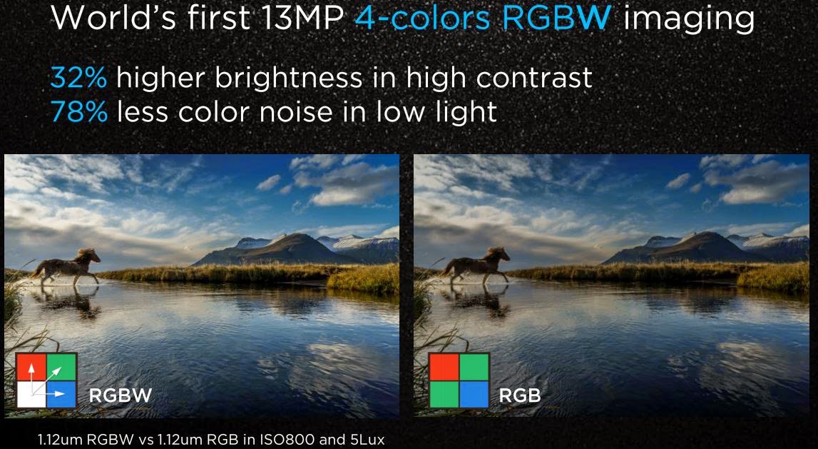
Huawei P8 flagship smartphone announced today features "a new philosophy for camera design leveraging a combination of hardware, software and proprietary algorithms to help users capture beautiful photographs, even in the worst lighting conditions."

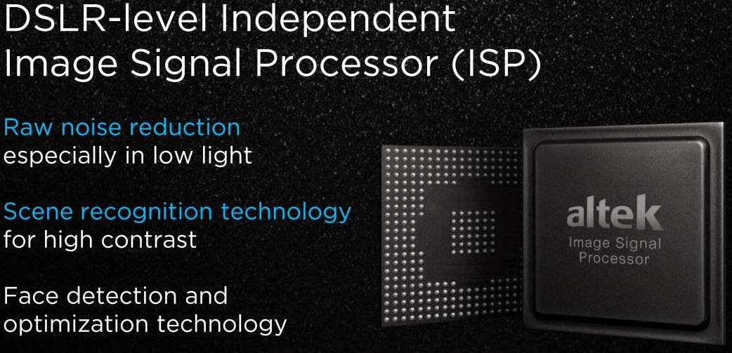
P8 camera sensor is claimed "The world’s first four-color RGBW sensor enhances brightness by 32 percent in high contrast lighting situations, reduces it by 78 percent in low light environments. DSLR-level independent image processor enabling noise reduction when shooting and intelligent detection of a high-contrast lighting environment." It's not clear what exactly makes Huawei camera "world's first RGBW," as other smartphones on the market already use sensors with white pixels in the array.

The camera also features "Industry-leading Optical Image Stabilizer technology up to 1.2°, enabling high-quality photos and videos, and managing camera shake so images are consistently sharp." For a very good image stabilizer one needs to have about 2-2.5deg range, but 1.2deg is not bad too.

About a half of Huawei P8 presentation is devoted to the camera (Youtube presentation is here):


Thanks to TS for the pointer!
Altek: Dual-lens Modules Become Mainstream smartphone Camera Solution

Altek: Dual-lens Modules Become Mainstream smartphone Camera Solution

Digitimes: Dual-lens modules are becoming a mainstream solution for smartphone cameras starting 2015, says Alex Hsia, chairman for Taiwan-based digital camera ODM and lens solution provider Altek. Smartphone vendors' adoption of dual-lens modules for cameras is motivated by product differentiation, as most smartphones are quite similar in screen, processor, memory capacity and operating system specifications, Hsia said.

Apple Acquires Array Camera Developer LinX

WSJ, Techccrunch: Apple has acquired Israeli array camera-technology company LinX Computational Imaging Ltd. Apple confirmed the acquisition with its standard statement when it has bought a company: “Apple buys smaller technology companies from time to time and we generally do not discuss our purpose or plans.”

The companies had been discussing an acquisition price of about $20 million, according to people familiar with the matter. LinX was founded in 2011. Co-founders and principal shareholders Ziv Attar and Andrey Tovchigrechko are industry veterans. Before starting LinX, Mr. Attar served as a senior optics specialist at Israeli defense company Rafael Advanced Defense Systems Ltd. Mr. Tovchigrechko led a team of algorithm developers at Samsung Israel.

Most of LinX web site has changed today and now shows very little info out of the rich content covered in the earlier posts here and here.

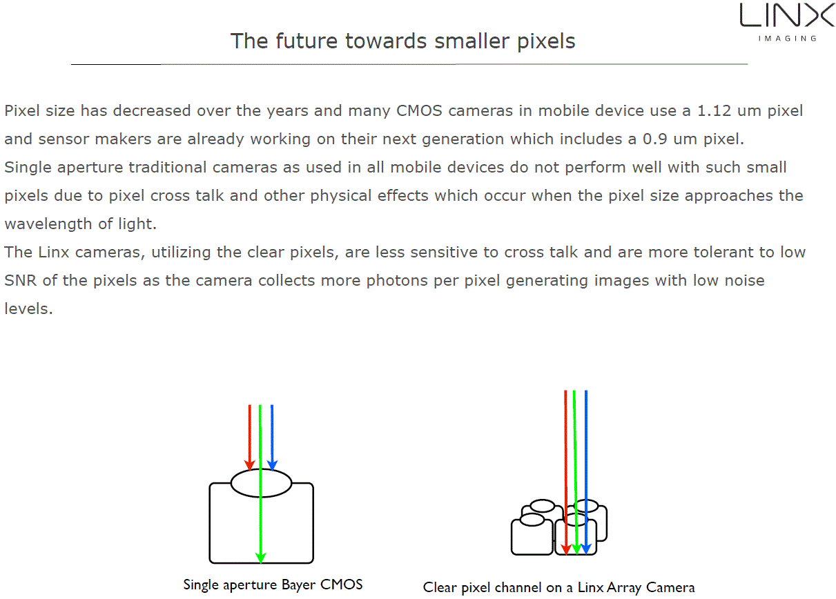
Few slides from the company presentation deck, now missing from its web site (sorry for too many pictures today):


Update: Globes reports "LinX had previously been in advanced talks to sell the company to both LG and Samsung and had even launched a successful pilot project with the latter but no agreement was ever reached on embedding the cameras into Samsung's smartphones."

Macrumors has uploaded the complete LinX June 2014 presentation on Sribd.
Movidius Raises $40M

Movidius Raises $40M

Movidius announces that it has raised $40 million in new funding. The investment was led by Summit Bridge Capital (a collaboration between Atlantic Bridge Capital and WestSummit Capital) and includes new contributions from ARCH Venture Partners and Sunny Optical Technology Group, as well as early investors including Atlantic Bridge Capital, AIB Seed Capital Fund, Capital-E, DFJ Esprit and Robert Bosch Venture Capital. The funding is said to be the most significant investment in a fabless semiconductor company in the past two years.

Movidius has pioneered an entirely new class of cost-effective, low power and high performance processors, software and development tools, and this platform enables our customers to implement visual sensing that aims to mirror human vision capabilities,” said Remi El-Ouazzane, CEO of Movidius. “This infusion of capital provides us with the resources to expand strategically, innovate constantly and extend our market leadership.

A promotional Vimeo video talks about the company and its markets:

Movidius from One Net Marketing on Vimeo.

Basler 3D ToF Camera Presentation

Basler kindly sent me a presentation on its new 3D camera with Panasonic ToF sensors. Few slides from the presentation:


Basler ToF camera has received Vision System Magazine's Gold Innovation Award at Automate Show in Chicago at the end of March.