BMW 3 Rear View Camera Teardown

EETimes publishes an article on BMW 3 Series rear view camera teardown with Omnivision's sensor inside. The estimated cost of the camera is between $50 and $75, while the price paid for the teared down device was $400.

The rear view camera board

Modern Image Sensor Testing Challenges

Formfactor and Advantest presentation "Can testers and probe cards keep up with speed requirements for image sensors?" at Semiconductor Test Workshop in San Diego, CA on June 8-11, 2014 talks about the high speed interface testing issues:

Sony Updates Xarina Roadmap

Sony has updated its web page on Xarina, the family of all-in-one HD image processors for security cameras. A support for 4K cameras is coming sometime in 2015:

Google Tango Project Tablets Feature pmd's 3D technology

PresseBox: Google’s Advanced Technology and Projects group (ATAP) is demonstrating their latest Project Tango Tablet Development Kits at Google I/O 2014 today. Now, for the first time, the tablets with integrated pmd-based depth sensors are shown publicly. Besides a motion tracking and a RGB camera the tablets utilize a pmd-based 3D ToF sensor to allow the tablet to sense its environment in space and motion. The ToF sensor used in the tablet has been jointly developed by Infineon and pmdtechnologies.

"We are proud that Google's ATAP group shows the world for the first time how our 3D technology is contributing to the addition of environmental awareness to mobile devices in a new and unique way. We also look forward to seeing what kind of amazing applications will be developed based on this tablet as the possibilities are endless in applications such as augmented reality, architecture, retail, gaming, and many more.", says Bernd Buxbaum, CEO of pmdtechnologies.


A Youtube video shows Project Tango evolution and possible applications:


Update: PMD publishes a short Youtube video of Google Tango tablet with PMD ToF camera inside:

Pixart Introduces CIS-based Heart Rate Monitor

Pixart Introduces CIS-based Heart Rate Monitor

PR Newswire: Pixart keeps looking for the unusual image-sensor based products. The company's PAH 8001 Heart Rate Monitor integrates a unique CMOS sensor with a LED in a single package. The PAH 8001 uses photoplethysmogram (PPG) technique which passes a green LED light wave into the skin and measures the response change caused by the absorption due to the pulsating arterial blood. The actual measurement is done using a small CMOS Pixel Array and the output data can be used to not only monitor heart rate, but also body stress level, etc.

The Pixart's PAH 8001 is said to be the industry's smallest form factor device with low power consumption. Human trial testing results with the PAH 8001 device closely matches the accuracy obtained using a Medical heart rate measurement system, but packaged in a tiny 3mm x 5mm module and consumes 1.5mA (typ). When used while performing a high impact activity such as running or jogging, the initial testing data shows the accuracy to be within +/-5BPM for speeds up to 8km/h.

"PixArt Imaging is the current market leader in optical mice, but the core technologies (CMOS imaging, optical and system integration) are now enabling the development of new and emerging innovative applications being introduced into the marketplace." said Dennis Lo, President, PixArt Imaging USA. "This heart rate monitor sensor is just the beginning of a line of healthcare monitoring solutions that we will be introducing this year."

Softkinetic and Melexis Collaborate on Automotive ToF Sensor

PR Newswire: SoftKinetic and Melexis announce the availability of their first ToF 3D sensor for automobile safety and infotainment markets. The MLX75023 sensor featurs SoftKinetic technology and manufactured in Melexis' automotive-grade CMOS mixed signal process. It's said to work in full sunlight and can be used for natural 3D gesture recognition and robust driver monitoring.

The MLX75023 features include:
  • QVGA resolution (320 x 240 pixel)
  • DepthSense TOF pixels
  • 1/3” sensor format (4.8 x 3.6 mm2)
  • High ambient light robustness, up to 120 Klux
  • Spectral response range 800-900 nm
  • Suitable for LED or laser illumination
  • Sensor modulation up to 40 MHz
  • Up to 600 fps raw image frame rate
  • Small glass BGA package
  • Ambient temperature range –40 to +105 degC

"Working together with Melexis we have now been able to create a sensor that is robust in full sunlight, perfect for the automobile environment," said Michel Tombroff, CEO of SoftKinetic. "We are excited about the multitude of possibilities with this sensor, and look forward to the ways car manufacturers will incorporate it into the design of their vehicles' cockpits and beyond."

"Our partnership has allowed us to be the first to provide 3D vision to the automotive safety and infotainment markets, and we are confident that these sensors will enhance life safety and change the way drivers and passengers enjoy the vehicle experience," said Françoise Chombar, CEO at Melexis.

Howard Rhodes' Presentation at IS 2014

Yole Developpement reviews Howard Rhodes, Omnivision's CTO, presentation at 2014 Image Sensor Conference in London, UK. The "The Future of CMOS Imaging" presentation shows stacked sensor as the next big thing and discusses the different stacking approaches, among other stuff:

Toppan-SMIC JV Begins 12-inch CFA & ML Production

Toppan-SMIC JV Begins 12-inch CFA & ML Production

PR Newswire: SMIC announces that the first 12" CFA & micro lens array production line in mainland China has been completed and put into production by Toppan SMIC Electronics (Shanghai) Co., Ltd. ("TSES"), a joint venture of SMIC and Toppan. Combined with SMIC's 12" CIS wafer production line, a full 12" CIS supply chain will be established in China.

"Building a 12" color filter & micro lens array production line is an pivotal step for SMIC to create IC manufacturing supply chain and implement differentiated strategy," said Dong Cui, EVP of SMIC Investment and Strategic Business Development. "With SMIC's front-end 12" CIS wafer manufacturing line in volume production and existing domestic back-end package capacity, SMIC will build the first complete 12" CIS supply chain in China covering all the processes of front-end, middle-end and back-end to support customers with differentiated offerings and a convenient one-stop service."

"TSES, invested jointly by SMIC and Toppan, is the first company in China to manufacture and sell color filter and micro lens array used for CIS. Its 8" production line has been put into volume production for many years. The new 12" production line will further extend SMIC and TSES's business scopes," said Mike Rekuc, EVP of SMIC Worldwide Sales and Marketing.
Open Access Papers

Open Access Papers

The new open access IEEE publication, IEEE Journal of the Electron Devices Society, which published Eric Fossum's pinned PD review, now publishes too more papers on photodiodes:

"Pixel Level Characterization of Pinned Photodiode and Transfer Gate Physical Parameters in CMOS Image Sensors" by Goiffon, V.; Estribeau, M.; Michelot, J.; Cervantes, P.; Pelamatti, A.; Marcelot, O.; Magnan, P.
Institut Suprieur de l'Aeronautique et de l'Espace (ISAE), Universite de Toulouse, Pyxalis

"Extraction and Estimation of Pinned Photodiode Capacitance in CMOS Image Sensors" by Chao, C.Y.; Chen, Y.; Chou, K.; Sze, J.; Hsueh, F.; Wuu, S.
TSMC

Thanks to DSSB for the link!
Mantis Vision Raises $12.5M from Strategic Investors

Mantis Vision Raises $12.5M from Strategic Investors

Marketwired: Mantis Vision announces a $12.5M strategic investment round from Qualcomm Ventures, Flextronics' hardware venture arm, Lab IX; Sunny Optical, and Samsung. Mantis Vision believes this strategic investment will accelerate its plans for shifting the 3D paradigm via its core MV4D technology platform.

"3D is as big a paradigm shift for mobile as was the introduction of the camera-phone, the type of change that only comes around once every decade. We now have the opportunity to deliver professional-grade 3D-enabled mobile devices and capabilities to the world," said Amihai Loven, CEO, Mantis Vision. "Our mission is to bring 3D to the masses, allowing users to create their own 3D content with ease. This strategic investment offers us the flexibility to expand quickly and strategically, as well as fuel adoption and engagement directly with consumer audiences worldwide."

Rambus Optimizes Conditional Reset Pixel

Rambus conditional reset pixel requires an ability to control reset on per pixel basis:


The company patent application US20140158863 "High Fill-Factor Image Sensor Architecture" by Michael Guidash proposes to combine column reset select line with the output bitline:

Sony Improves IR Response of its BSI Sensor

Sony announces 3.21MP 2.5um BSI pixel CMOS sensor IMX123LQT with improved NIR sensitivity for industrial applications. "Sensitivity in the near infrared range has been increased to 1.5 or more times that of existing models by applying technical know-how for improving sensitivity in the near infrared range developed for front-illuminated structures to the pixels of an industry-leading back-illuminated structure."

The sensor features WDR mode based on "DOL (digital overlap) drive: This function outputs up to three frames of images alternately on each line. It requires a dedicated ISP, but provides advantages such as improved characteristics in low-light environments compared to conventional WDR that uses multiple frame set output. (See photograph 3.) Multiple DOL drive settings are provided to enable control and data reception in accordance with the ISP used."


Additional WDR features are:
  1. 14-bit ADC enables a good DR from a single image
  2. Multiple frame set output function. The exposure time and the gain can be set separately for each frame. This function helps to realize WDR functions, and can also be applied to applications such as bracket shooting.
  3. Function that combines two images with different exposure times inside the image sensor and outputs the synthesized image. This function is suited to applications that aim to easily realize WDR when there is no function for combining multiple frames on the ISP side

RF Testers Meet Image Sensors

As MIPI speed follows the image sensor frame rate advances and reaches higher Gbps rates, Agilent comes with S-Parameter test suite adapted for MIPI channel tests:

Amazon Fire Phone Uses 4 IR Cameras for 3D UI

The Verge, Mashable: Amazon Fire Phone uses four front-facing IR cameras to create a 3D user interface: "Perhaps the most useful application shown off so far is simply tilting the phone to scroll through a web page like The Washington Post or to page through a Kindle book. Of course, we've seen other tilting features before and they've a lot to be desired, but Amazon's demo seems to make these features seem far better than previous attempts. The question will be whether or not the extra processing power and potential battery life drain to run these multiple cameras will be worth it."

Jeff Bezos presents 3D UI features
Dual Aperture Announces JV with KAIST

Dual Aperture Announces JV with KAIST

PR Newswire: Dual Aperture, Inc. announces a joint venture with the Center for Integrated Smart Sensors (CISS) that will more than double the engineering resources dedicated to commercializing Dual Aperture's 3-D imaging technology. Dual Aperture's technology is based on its 4-color sensor that is equipped with a dual aperture design, which is comprised of RGB and IR pixels. The sensor also uses separate apertures for the respective RGB and IR pixels, thereby capturing data for two distinct images -- one each in the RGB and the IR spectrums -- with different levels of sharpness to generate real-time 3D depth information.

Professor Chong-Min Kyung, CEO of CISS and Professor at KAIST, adds, "CISS receives collaboration proposals from all over the world and when we examined Dual Aperture's technology, we jumped at the opportunity to build on what we believe to be truly disruptive technology for smart cameras and smart sensors. We are extremely excited to work with Dual Aperture for the advancement of RGB-IR technology."

A Vimeo video shows gesture recognition application based on the company's technology:

Dual Aperture Gesture Control from Dual Aperture on Vimeo.

Tessera Brings Back Fotonation Brand

Tessera Brings Back Fotonation Brand

FotoNation, a wholly owned subsidiary of Tessera, announces that it will once again operate under its original FotoNation name. Fotonation's software is said to be inside of more than 60% of global tier-1 smartphones. FotoNation will operate as a distinct identity of parent company Tessera Technologies.

FotoNation is now taking its advances in smartphone imaging algorithms into the growing automotive, surveillance, security, and augmented reality markets. “All manner of machines, as well as the cameras inside them, are getting smarter. As their computational power increases, the opportunity for advanced imaging technologies also increases,” said Petronel Bigioi, VP of Engineering at FotoNation. “We are enabling cars to tell the difference between sleepy and wakeful drivers, security cameras to know who is accessing a secure environment, smartphones to perform biometric authentication, and a wealth of new applications in the growing wearable-computing space.

ULIS Announces 0.7MP/100fps 200mW IR Imager

ALA: ULIS, a subsidiary of Sofradir and GE Equity, announces the Pico1024E GenII, an energy-efficient thermal image sensor for military applications.

"ULIS’ megapixel Pico1024E GenII meets the challenges in thermal image sensors for military applications that need to offer new capabilities and perform at very high standards, while operating with minimum energy," said Jean-Francois Delepau, managing director of ULIS. "Pico1024E GenII has already stimulated interest from defense equipment customers. Its performance pushes the standards in image crispness, frame rate frequency and low power consumption to the highest levels. We expect Pico1024E GenII to open up new possibilities in the future development of thermal imaging systems."

Pico1024E GenII, a 1024 x 768 17um pixel thermal image sensor, is able to maintaining power consumption at the lowest levels (200mW) at frame rate of 100fps. This is close to double the frame rate frequency for this category of megapixel thermal image sensor. A progress in lowering the power consumption down to 200mW put it ahead of competing products requiring two to three times more electrical power. Major upgrades to Pico1024E GenII consist of higher thermal sensitivity of lower than 50mK, offering 15 per cent additional thermal sensitivity over the previous generation.

BAE is First to Commercialize 12um IR Pixel Imager

BAE Systems: Developed for a new class of compact and low-cost imaging systems, BAE TWV640 thermal camera core is based on the first commercially available uncooled 12um pixel. Reducing the pixel size from 17um to 12um is said to allow imaging system manufacturers to reduce lens size by 50% and decrease optics costs by 20%.

"As the first to deliver a 12-micron thermal camera core, we’re providing our customers a tremendous competitive advantage, helping them drive down system costs while providing superior imagery typically associated with our MicroIR products," said Christian Rodriguez, business development at BAE Systems. "Our TWV640 module empowers our customers to create and deliver a new generation of affordable, compact, thermal imaging systems for a broad range of applications."

Further advancing the technology developed for the 17um MIR640 thermal camera core, the TWV640 module is optimized to provide affordable thermal imaging performance in a compact, low-power solution. The TWV640 camera core captures VGA images at 60Hz to observe dynamic environments revealing details that competitors’ 30Hz offerings miss, while also eliminating the disorientation that comes from using slower video.

Compatible with off-the-shelf lenses from leading optics providers and using standard interface protocols like USB, NTSC and CameraLink, the TWV640 module is a drop-in 640x480 thermal camera core designed for makers of commercial, civil and military thermal imaging solutions.

Curved CCDs from Andanta

As Sony presents its curved CMOS sensors, one has to mention that Olching, Germany-based Andanta has first shown its commercially available curved CCDs in 2012. The 2013-dated document presents cylindrically curved FSI devices as standard products, while the spherical ones are available on request:


The company says: "The curvature of the image sensor can be designed as a one-dimensional cylindrical curvature or as a two-dimensional spherical curvature (convex or concave). As part of a customized project, scientific front illuminated 4k x 4k (16 Mpixels) - image sensors with convex and concave surfaces have already been realized. The applied vacuum technology (also usable on back side illuminated CCDs) has not created any measurable increase in detector noise or the number of cosmetic defects compared to the conventional flat image sensor with identical electro-optical properties. Cyclic mechanical stress testing has shown good results as well."

Smart Doors - New Market for 3D Cameras

IEEE Spectrum shows what might develop into a mass market for 3D cameras - smart sliding doors, presented by University of Electro-Communications, and Hokuyo Automatic Co. at 2014 IEEE International Conference on Robotics and Automation (ICRA) in Hong Kong. A Youtube video explains the idea:

Sony Curved Image Sensor Presentation

IEEE Spectrum reports from VLSI Technology Symposium in in Honolulu, Hawaii on Sony curved image sensor presented by Kazuichiro Itonaga, device manager with Sony's R&D Platform in Atsugi-shi, Japan:

"Itonaga gave few details on the process the team used create the curved CMOS chips. He said that a machine was used to bend the CMOS sensors and that they were backed with a ceramic to stabilize them after bending. It was also unclear how much the chips were curved, although Itonaga said that they did achieve the same level of curvature found in the human eye.

Two chips were reported. One, which measured some 43 millimeters along the diagonal, is a full-size chip for digital cameras. The other is a smaller chip, more suitable for mobile phones, which measured 11 mm along the diagonal and boasts smaller pixels. The team integrated the curved image sensor with a lensing system and showed an image that seemed to be quite good, although it wasn't displayed alongside an image taken with an equivalent flat sensor for comparison.
"

"The team has made somewhere in the vicinity of 100 full-size sensors with their bending machine. "We are ready," Itonaga said."

Sony curved sensor

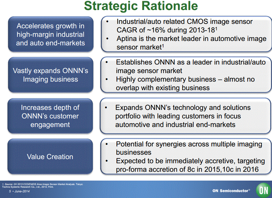
ON Semi's Presentation on Aptina Acquisition

ON Semiconductor publishes a transcript its conference call script and investor presentation on the Aptina acquisition:


There is a clarification message I got from Aptina: "Many are wondering about mobile. Consumer & Mobile are a key businesses for us and in the top 5 businesses for ON. We are committed to this business as long as it generates returns (which it is)."

High Performance Silicon Imaging Book

Woodhead Publishing release a new book "High Performance Silicon Imaging" written by a number of world's experts in image sensor design and applications, and edited by Daniel Durini (Fraunhofer Institute, Germany). Here is the list of topics:
  • Fundamental principles of photosensing
    D. Durini and D. Arutinov (Fraunhofer Institute, Germany)
  • Operational principles of silicon image sensors
    D. Durini and D. Arutinov (Fraunhofer Institute, Germany)
  • Charge coupled device (CCD) image sensors
    M. Lesser (University of Arizona)
  • Backside illuminated (BSI) complementary metal-oxide-semiconductor (CMOS) image sensors
    A. Lahav, A. Fenigstein and A. Strum (TowerJazz)
  • Circuits for high performance complementary metal-oxide-semiconductor (CMOS) image sensors
    B. Choubey (University of Oxford, UK), W. Mughal and L. Gouveia ( University of Glasgow, UK)
  • Smart cameras on a chip: using complementary metal-oxide-semiconductor (CMOS) image sensors to create smart vision chips
    D. Ginhac (Université de Bourgogne, France)
  • Complementary metal-oxide-semiconductor (CMOS) image sensors for mobile devices
    R. J. Gove (Aptina)
  • Complementary metal-oxide-semiconductor (CMOS) image sensors for automotive applications
    C. De Locht and H. van den Broeck (Melexis, Belgium)
  • Complementary metal-oxide-semiconductor (CMOS) image sensors for use in space
    J. Bogaerts (CMOSIS, Belgium)
  • Complementary metal-oxide-semiconductor (CMOS) sensors for high-performance scientific imaging
    R. Turchetta (Rutherford Appleton Laboratory)
  • Complementary metal-oxide-semiconductor (CMOS) sensors for fluorescence lifetime imaging (FLIM)
    R. K. Henderson (University of Edinburgh, UK), B. R. Rae (ST, UK) and D.-U. Li (University of Strathclyde, UK)
  • Complementary metal-oxide-semiconductor (CMOS) X-ray sensors
    A. Strum and A. Fenigstein (TowerJazz)
  • Complementary metal-oxide-semiconductor (CMOS) and charge coupled device (CCD) image sensors in high-definition TV imaging
    P. Centen (Grass Valley Nederland)
  • High-performance silicon imagers and their applications in astrophysics, medicine and other fields
    S. Nikzad (JPL, CA)

On Semi to Acquire Aptina for $400M

Business Wire: ON Semiconductor signes a definitive agreement to acquire Aptina Imaging. The high-performance CMOS image sensors for automotive and industrial markets are said to be the key areas of strategic focus for ON Semi. According to TSR, the worldwide demand for image sensors for automotive and industrial applications is expected to grow at annual compound rate of 16% between 2013 and 2016.

ON Semi will pay approximately $400M in cash to acquire Aptina Imaging, subject to customary adjustments at closing. The acquisition will be funded by available cash on ON Semi’s balance sheet and its existing revolver credit facility.

"The pending acquisition of Aptina enables us to accelerate our growth in the attractive automotive and industrial end-markets by leveraging Aptina’s highly differentiated imaging technologies in conjunction with our wide sales reach and strong operational capabilities," said Keith Jackson, president and CEO of ON Semiconductor. "The addition of Aptina vastly expands our scale and capabilities in image sensors and establishes us as a leader in image sensors for industrial and automotive related applications. I am excited about the possibilities that this transaction presents for both companies."

Based on unaudited results, Aptina’s revenue for last twelve months ending on May 29, 2014, was approximately $532 million with gross and operating margins of approximately 29% and 3%, respectively. ON Semiconductor currently intends to report operational results for Aptina and other image and optical sensor businesses in a separate reporting segment. The transaction has been approved by ON Semi’s and Aptina’s boards of directors and is expected to close during Q3 2014.

Update: Seeking Alpha publishes analyst's comments on the deal.

Update #2: EETimes publishes an article on ON acquisitions history and analyst responses to Aptina purchase. The article quotes Yole table of market shares in 2012, where the top 3 vendors control 58% of the $6.9B market:

Market shares in 2012,
according to Yole Developpement

Ziptronix and EVG Achieve Sub-Micron Stacked Wafers Alignment

EETimes: Ziptronix and EV Group (EVG) announce they have achieved submicron post-bond alignment accuracy on customer-provided 300mm DRAM wafers using Ziptronix's DBI Hybrid Bonding technology on an EVG Gemini FB production fusion bonder and SmartViewNT bond aligner. This approach can be used to manufacture fine-pitch 3D ICs for a variety of applications including advanced stacked image sensors.

Ziptronix Direct Bond Interconnect (DBI) Hybrid Bonding is a conductor/dielectric bonding technology that includes a variety of metal/oxide and/or nitride combinations, does not use adhesives and allows for strong, room temperature dielectric bonding, low temperature conductive bonding and finer-pitch interconnect over Cu/Cu or other metal bonding because the bond occurs between both the dielectric and the conductive surfaces, which effectively bonds the entire substrate interface area. DBI Hybrid Bonding can be used at the die or wafer level; however, wafer-level bonding enables a great cost benefit by bonding all the dice at once.

Truesense Acquisition Story

Truesense Acquisition Story

Rochester Business Journal publishes a story on Truesense acquisition by ON Semi. Few quotes:

"Eight prospective buyers emerged to purchase Truesense, touring the company’s facilities and evaluating its online data box, said Christopher McNiffe, previous CEO of Truesense Imaging and current vice president of the image sensor business unit of ON Semiconductor... Roughly 300 people now report to McNiffe, including 50 people who work near Brussels, Belgium, a dozen in Bangalore, India, and 10 in Santa Clara, Calif."

"Under ON Semiconductor’s watch, Truesense Imaging is expected to grow, officials say."

"I see the real power of this acquisition being we have the best of both worlds," McNiffe said. "So now we can go in to a customer and we can say: ‘Here’s a broad portfolio of high-performance image sensors. Which one of these is the best fit for what you’re trying to do?’ That’s something that no one else in our industry is able to do right now."

Sony Semiconductor Business Update

Sony releases a flyer updating its semiconductor business data, with image sensors shown separately. Most of the data was already published in the 2013 Annual Report.

TowerJazz and Genoray Announce 100um Pixel X-Ray Sensor

TowerJazz and Genoray Announce 100um Pixel X-Ray Sensor

Business Wire: TowerJazz and Genoray announces a successful development of a CIS for medical diagnostic devices such as X-ray equipment, fluoroscopy and radiography in TowerJazz’s 0.18um CIS stitch process. The novel device which has a 100um pixel size and has a special feature to control the sensitivity of the pixel which can be applied in various types of medical equipment such as surgical C-Arms and portable X-ray machines.

This new device is a CIS detector whereas the existing market uses a silicon TFT type sensor. The advantage of CIS compared to TFT is that CIS uses active pixels so it obtains the image with less noise and helps minimize X-ray radiation exposure which is currently the biggest issue in the industry. Furthermore, Genoray’s single detector supports both CT mode and Panorama mode while the existing products in the market only support one by one (CT supports only CT mode, Panorama supports Panorama mode only). This means that by providing multi-functions through one detector, Genoray can satisfy customers who need both modes with a less expensive price point; a competitive advantage of this product.

Mantis Vision's Structured Light 3D Camera Used in Google's Project Tango Tablets

Marketwired: Mantis Vision confirms that its MV4D 3D camera is used in Google's Project Tango tablet. Mantis Vision camera consists of flash projector hardware components and includes structured light-based depth sensing algorithms. "3D represents a major paradigm shift for mobile. We haven't seen a change this significant since the introduction of the camera-phone. MV4D allows developers to deliver 3D-enabled mobile devices and capabilities to the world," said Amihai Loven, CEO, Mantis Vision. "This partnership with Google offers Mantis Vision the flexibility to expand quickly and strategically. It will fuel adoption and engagement directly with consumer audiences worldwide. Together, we are bringing 3D to the masses."

"We are excited about working with partners, such as Mantis Vision, as we push forward the hardware and software technologies for 3D sensing and motion tracking on mobile devices," said Johnny Lee, Technical Product Lead at Google.

A Youtube video demos the company's technology:


In another video Mantis CEO discusses his future vision:


Yet another Youtube video by Google introduces Project Tango tablet with Mantis camera inside:

Google Announces PMD as a Project Tango Partner

Google’s ATAP group (Advanced Technology and Projects group, a former part of Motorola Mobility) announces, that PMD is one of the technology partners in Project Tango integrating a 3D camera in a smartphone and tablet form factors. The 3D ToF image sensor belongs to IRS 10x0C chip family developed by PMD in collaboration with Infineon and featuring PMD's Suppression of Background Illumination (SBI) to improves the sensor chip’s DR for indoor and especially for outdoor operations. PMD 3D camera comes in place of Primesense one used in the early version of the project.

GigaOm reports that Google Tango tablet becomes available to developers later this month and costs $1,024.

Thanks to JZ for the news!

Google video talks about the Tango platform uses:

LinX Imaging Announces Array Camera for Mobile Applications

Business Wire: "The image quality of mobile cameras has reached a dead end. Device makers are striving to differentiate using imaging capabilities but the pixel size race has ended and next generation cameras do not reveal any dramatic improvements," says LinX Computational Imaging Ltd.. The company reports that it has successfully developed miniature multi-aperture cameras for mobile devices with nearly half the height of a standard mobile camera and are capable of creating stunning color images and high accuracy depth maps. The engineers at LinX have solved all problems associated with combining multiple images captured from different points in space such as registration errors and occlusion related artifacts which are seen on competing technologies, so that LinX cameras are artifact-free, even when objects appear at very short range.

LinX software also creates a true depth information on high contrast objects and on near flat surfaces, such as walls, which are traditionally considered difficult for passive stereo systems. With its partners, LinX has developed a variety of products ranging from arrays of two, three, and four cameras in various configurations and sizes, some with autofocus and others without. The technology is said to be ready for integration into the current generation mobile devices:


LinX technology is said to have many advantages over traditional mobile photography:

  • A larger sensor requires a longer lens. Therefore, by replacing one large sensor with two or more smaller ones, we reduced the height of our device by a factor of 1.4 to 2
  • Sensitivity to light increases by a factor of 3 by using a monochrome sensor
  • Noise levels are dramatically lower
  • The effective array camera resolution is similar to the single aperture camera in high light
  • Performance and image quality in low light are extraordinary
  • Allowing a fast exposure at indoor standard lighting conditions of 100-200 lux which assures crisp images free from motion blur
  • The multi-aperture camera creates a real-time, high-quality distance map

30-page LinX technology presentation shows many comparison pictures with iPhone 5s and Galaxy s4 cameras, many of them in low light:

Ambarella Reports Quarterly Results

Ambarella Reports Quarterly Results

GlobeNewswire: Ambarella reports that revenue for its fiscal quarter ended April 30, 2014 was $40.9M, up 21% from $33.9M a year ago. GAAP gross margin was 62.5%, compared with 63.9% for the same period a year ago. GAAP net income for the first quarter of fiscal 2015 was $5.3M, compared $4.7M a year ago.

"We are very pleased with the financial results of our first fiscal quarter of 2015," said Fermi Wang, president and CEO. "During the first quarter we achieved revenue of $40.9 million, up 21% from the same period last year, driven by continued growth in our IP security camera business. We believe the expanding markets for innovative, high definition professional and consumer cameras will continue to give us the opportunity to grow our revenues in the year ahead."

Apple Applies for Li-Fi-Optimized Image Sensor Patent

Apple patent application US20140125852 "Optical demodulation using an image sensor" by Richard Baer, Michael Malone, Ting Chen, and David Amnon Silverstein proposes two-mode image sensor. The first mode is a regular image capture, while the second one is optimized for the lighting LED-based data communication (Li-Fi). In Li-Fi mode, "the integration interval for the image sensor is set to less than two row periods, preferably close to one row period, without regard to the exposure data if the data capture mode is selected.

An analog gain may be increased to as large a value as possible in data capture mode. All pixels in a row may be summed before analog to digital conversion in data capture mode. An image sensor frame period may be set according to a signaling frame period of an illumination modulation data transmission in data capture mode.

The controller may further causes data to be inverted from frame to frame and decoding of the difference of two successive frames if the data capture mode is selected. The controller may further causes defocusing of an optical system that forms an image on the image sensor if the data capture mode is selected.
"

Rumor: ST Supplies SPAD-based ToF Autofocus for LG G3 Smartphone

The newly announced LG G3 smartphone features an intriguing piece "Laser Auto Focus measures the distance to the subject using laser technology. Laser Auto Focus allows for improved focusing speed and object detection in low-light situations." I was told that this AF utilizes STM's SPAD-based ToF range finder. A similar SPAD device is also used in a low-end Bosch laser distance measurer PLR15.

If true, the SPAD ToF technology finds its way to more and more mass market devices: first to ST proximity sensor, then to Bosch distance meter, and now to LG G3 flagship smartphone.

Omnivision Launches Industry's Lowest Power 1080p60 Sensor

PR Newswire: OmniVision announces the OV2740, an ultra-low power PureCel image sensor consuming only 90mW when recording 1080p HD video at 60fps. The OV2740 is said to be the lowest power 1080p60 image sensor currently on the market. Built on a 1.4um BSI pixel, the OV2740 PureCel image sensor achieves a 50% improvement in FWC and a 30% improvement in sensitivity over the previous generation OmniVision sensors. The OV2740 features staggered HDR mode with minimized motion artifacts.

The OV2740 is the only 1080p HD image sensor announced to date that features light-sensing mode (LSM) and ultra-low power mode (ULPM), enabling advanced features such as motion detection or gesture control. Additionally, the sensor is stereo ready with frame synchronization to support a host of depth perception applications.

The OV2740 fits into a 5 x 5 x 3 mm module. It is currently sampling and is expected to enter volume production in Q3 2014.