Congnivue Image Cognition Processor Targets Low Power Devices

Congnivue Image Cognition Processor Targets Low Power Devices

PRWeb: CogniVue announced the ability of its Image Cognition Processor (ICP) to support always-on vision applications like gesture recognition, face and eye detection in low power smart wearable devices at power levels of ~1mA, enabling vision apps to run for many days as opposed to hours. CogniVue’s APEXTM ICP are said to be better than 100x performance per power vs conventional processing architectures for embedded vision applications. That significant performance per power advantage is paying off in the rapidly accelerating market of smart wearable devices. This advantage will grow as next-generation APEX cores are announced by CogniVue later in 2014.

One of Cognivue customers, NeoLAB Convergence went to production with the Neo 1 smart pen, said to be the smallest and longest lasting smart pen in the market. The pen uses CogniVue 1st generation APEX-based technology and an image sensor both operating at 120fps to render hand writing and hand drawings in real time to a smart phone or tablet or server wirelessly with no perceived delay. It does this at very low power levels, enabling this battery-powered device to last for weeks on a charge. NeoLAB engineers dramatically increased battery life compared to the competition and they were able to go from design start to prototype in as a little as 6 months using CogniVue’s comprehensive software development kit.

A Vimeo video presents the company positioning and technology:

LFoundry Rousset Fab Might Return to Life as Thin-Film Vision Sensor Facility

EETimes-Europe, EETimes report that the Commercial Court of Paris, France is considering 12 bids for the bankrupted LFoundry wafer fab in Rousset and its assets; one from General Vision Inc. and 11 others from brokers who wish to acquire the fab equipment and sell it on.

General Vision (Petaluma, CA) is a US company led by expatriate French expects in computer vision and neuromorphic computing and which includes Philippe Lambinet, formerly a corporate strategy officer at STMicroelectronics NV and general manager of ST's digital sector. General Vision is proposing to use the Rousset fab to manufacture neuromorphic chips and image sensors on glass substrates in a joint technology development with Japanese Asahi Glass, under a project call NeuroMem. The proposed chips could include a million neurons in a system that would function like the human visual system and recognize objects in visual inspection and robotic applications. General Vision has presented its plan to former employees at Rousset and said that if the liquidator accepts its proposal that it would need 120 employees by the end of 2014. Over the time General Vision hopes to expand its neuromorphic products manufacturing and return the site to the levels of employment when it was shuttered.

Stereo 3D Platforms

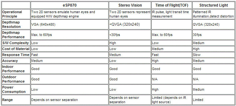
There are two almost simultaneous announcements of the stereo 3D camera platforms. One is Erton's Eagle Eyes 3D depth mapping platform based on eSP870 3D Depth-Map Camera Controller announced a year ago. Etron compares it with other depth sensing approaches:


Another 3D depth mapping announcement comes from Duo3D presenting AudioSight - a software-based solution turning stereo camera into a depth mapping device. The company's Youtube video demos the software capabilities:

Omnivision Reports Quarterly and Yearly Results

Omnivision Reports Quarterly and Yearly Results

PR Newswire: OmniVision reports financial results for the fourth quarter of fiscal 2014 that ended on April 30, 2014. Revenues for the quarter were $331.0M, as compared to $352.0M in the previous quarter, and $336.2M a year ago. GAAP net income in the last quarter was $15.1 million, as compared to net income of $30.6M in the previous quarter, and $8.9M a year ago.

Revenues for the fiscal year ended April 30, 2014 were $1.5B, as compared to $1.4B in fiscal 2013. GAAP net income for fiscal 2014 was $95.0M, as compared to income of $42.9M a year ago.

GAAP gross margin for the last quarter was 20.1%, as compared to 19.6% in the previous quarter and 17.5%a year ago. The increase in gross margin was primarily attributable to the introduction of newer and lower cost products into our shipment mix.

The Company ended the period with cash, cash equivalents and short-term investments totaling $450.9M, an increase of $57.9M from the previous quarter.

"We are pleased to conclude our fiscal 2014 on a high note. Our financial metrics have continued to improve, with better gross margin, higher cash balance, and lower inventories. We have made meaningful progress on multiple fronts, including the diversification of our revenues into multiple geographies, especially in Asia, and the strong growth in our emerging automotive and security markets," said Shaw Hong, CEO of OmniVision. "We are also working on new technologies and applications in our core and emerging markets that have the potential to substantially enhance our market position over the longer term."

The company expects revenues for the next quarter will be in the range of $360M to $400M.

Toshiba Announces New Image Recognition Processor

Business Wire: Toshiba expands its line-up of image recognition processors in the TMPV750 (Visconti) series with the launch of TMPV7502XBG, a small package (11mm × 11mm) and low power consumption (Typ. 0.6W) processor for small-size camera modules. Sample shipments start now, with mass production scheduled to start in November, 2014.

The new product can be applied to driver assistance systems that recognize vehicles and pedestrians in images captured by a vehicle’s rear view monitor and electronic mirror. It can also handle intelligent camera functions in diverse Smart Community related applications, including alarm systems using surveillance cameras on roads and at intersections, and image-based air-conditioning and lighting management systems in buildings.

Calls for Image Sensor Papers

Calls for Image Sensor Papers

CNES, AIRBUS DEFENCE&SPACE, THALES ALENIA SPACE, SODERN and ISAE announce a workshop focused on image sensors optical interfaces, which will be held in Toulouse on November 27, 2014 as a part of the Optics & Optoelectronics Technical Expertise Centers (CCT). The workshop is coupled with “Radiation Effects on Optoelectronic Detectors” workshop which will be held
the November 26. The two workshops will share the poster session and the cocktail.

Papers are solicited in the following areas:

Quantum efficiency/reflectivity improvement:
  • Backside Illumination (Back side surface treatment, …)
  • Wafer thinning
  • Microlenses (inside process flow or back end process)
  • Wave guides
  • Anti-reflective coatings
  • Black coatings
Spectral range/polarization selectivity:
  • Filters (colours, multiple nodes…)
  • Polarizers
  • Plasmonic wave guide
  • Integrated optical systems (Fabry Pérot…)
Basic Mechanisms of Radiation Effects on Optoelectronic Detectors:
  • Single Event Effects
  • Displacement Damage Effects
Radiation Effects on Optoelectronic Detectors Performances:
  • Ground Irradiation Tests
  • In-flight Results
  • Impact of Performance Drift on Satellite Performances
Radiation Test Methodology and Facilities:
  • Test Guidelines, Qualification Plan
  • Radiations Facilities
  • Characterization Procedures
Radiation Tolerances of Optoelectronic Detectors:
  • Mitigation Techniques
  • Radiation Hardened Design and Technology
  • Specific Operation Modes

Schedule:
October 3rd: Dead line for abstract submission
October 31st: Paper selection
November 3rd: Final programme
November 21st: Deadline for registration
November 26-27: Workshops

Organization committee:
Cédric VIRMONTOIS
Jacques LOESEL
CNES
Olivier SAINT-PE Airbus Defence and Space
Christophe RENARD Thalès Alenia Space
Vincent GOIFFON ISAE
Dominique HERVE SODERN

IEDM too announces a call for papers. This year a special focus session will be devoted to "Novel Devices for Specialty Imaging Applications." The deadline for submissions is June 23.

NHK Shows 133MP 8K Video Sensor

Tech in Asia got an early look at NHK open house exhibition, scheduled to open on May 29. One of the achievements is 133MP image sensor for 8K video cameras:


NHK also schedules a special lecture on bright future for 8K cameras for endoscopic applications.

Update: NHK publishes a flyer of the new sensor, showing its Bayer CFA:


Update #2: Gigazine publishes NHK poster saying that the sensor's speed is 60fps at 12b ADC resolution:


imager.no-mania.com speculates that the sensor is designed by Forza.

Update #3: NikkeiBP posts explanations on how 133MP resolution is used. The reason for the increased resolution is that 33MP needs to be maintained in each of RGB channels.
Aptina Buys CFA Manufacturing Assets from Micron

Aptina Buys CFA Manufacturing Assets from Micron

Business Wire: Aptina is to acquire CFA processing and probe imaging assets from Micron. In addition, Aptina will lease from Micron the Nampa, Idaho fabrication facility known as Fab 9D where the CFA processing is located. The purchase is expected to close in Q3 2014.

"Our growing revenues and strong financial position have enabled Aptina to purchase these assets and add great people which gives us a strategic advantage in the marketplace," said Phil Carmack, CEO of Aptina. "Our ability to tightly integrate the entire R&D cycle accelerates innovation and enables us to uniquely support our customers."

"The operating advantages of this deal will flow directly to the bottom line," said Tony Alvarez, Chief Operating Officer of Aptina. "The ability to innovate, such as we have done with Aptina Clarity+ technology, and customize CFA will drive growth opportunities in all of our market segments including automotive, mobile and surveillance."

Aptina's blog also publishes Q&A session with Tony Alvarez, COO, Jeff Mendiola, VP of Operations, and Terry Gilton, VP of Advanced Technology, with more details on the acquisition:

Question: Could you share an example where these capabilities help Aptina innovate?
Terry: The best example of Aptina’s prowess in the pixel optical stack development is (Aptina) Clarity+ technology. We would have not succeeded with this program without being very closely involved in the CFA process development and materials evaluations. For the future there are some very unique ideas that we can realize quickly with the CFA/ML teams like super small pixels, new color/material combinations, uniformity improvements and a few others that we don’t want anyone to know about yet!

Sony Announces 20.48MP/22fps CMOS Sensor and 1.45MP/45fps CCD

Sony announces IMX183CQJ, a 1-inch 20.48MP CMOS sensor based on 2.4um BSI pixels. It appears to be a version of the 1-inch sensor used in a number of recent Sony digital cameras and camcorders. Its full resolution speed is 22fps in 12b mode and 24fps in 10b mode:


Sony also announces two 2/3-inch 1.45MP CCDs, the ICX825ALA (black and white) and the ICX825AQA (primary color filter), for industrial applications. The CCDs feature an improved version of 6.45um EXview HAD CCD II pixel, compared below with the older version in ICX825AL and ICX825AQ CCDs:

Measured at 850nm wavelength
Himax Imaging Update

Himax Imaging Update

Seeking Alpha publishes Q&A session from Himax Q1 2014 earnings call. Few interesting quotes:

Jerry Su – Credit Suisse AG:

Is there a significant turnaround on your on several subsidiaries specific non driver – non-driver product lines?

Jackie Chang, CFO:

"Yes, LCOS company and also the Himax Imaging Technology that is the CMOS imaging sensor region that is still losing money. But we do expect one or both of them breaking even or be profitable this year."

Daniel A. Heyler – Bank of America Merrill Lynch:

Could you elaborate on the products, you just mentioning eight megapixel. Is that a BSI product – BSI technology or is that going to start on a FSI.

Jordan Wu, CEO:

The major BSI product we’re launching eight megapixel, which is really getting enjoying growing popularity design wise with customers... And later in the year we are going to launch around 1 megapixel BSI sensor for laptop and tablet, which is a full HD sensor. So that will likely be our second BSI product.

Daniel A. Heyler – Bank of America Merrill Lynch:

So is the eight megapixel BSI, is that currently shipping in volume or is that a third quarter ramp?

Jordan Wu, CEO:

No, it’s a third quarter thing, starting of third quarter. It’s going through design stage.

Daniel A. Heyler – Bank of America Merrill Lynch:

And is that on 12-inch wafer or is that going to be on 8-inch because I know capacity is pretty tight on 8-inch?

Jordan Wu, CEO:

No, it’s 8-inch, but TSMC has – we will agree upon to capacity reservation with TSMC. So I think we all can.

Aptina Proposes to Turn Clear Pixel into Yellow

Aptina's patent application US20140125838 "Imaging systems with modified clear image pixels" by Jeffrey Mackey, Gershon Rosenblum, and Alexandre Dokoutchaev proposes an improvement over the previously published Clarity+ application. The necessity for the improvement is explained as: "Some imaging systems replace the green color filters in the standard Bayer mosaic pattern by a non-absorbing clear material. This type of clear pixel can boost the sensor light sensitivity by a factor of more than two, thereby significantly improving the medium and low-light performance. However, this type of color scheme is partially subtractive and therefore can require the use of relatively high color correction coefficients. In addition, the high sensitivity of the clear pixel can result in a color channel imbalance that is typically corrected using relatively high white-balance coefficients. Thus, if care is not taken, proper color correction using these types of color correction and white-balance coefficients can result in an enhancement of pixel noise."

The solution is to modify the clear pixel: "Image pixels 190 may include modified clear pixels. For example, some of pixels 190 may include color filter elements formed from transparent material with a color additive such as a yellow pigment or other similarly shaded pigment or dye. The pigment may be added to the transparent color filter element material in concentrations configured to give desired spectral filtration qualities to an otherwise uniformly transparent color filter array pixel."

The processing pipeline with Clear pixel modified into Yellow is quite similar to the original, where C (clear) is changed to Y:

Google Too Files Array Camera Application

Google patent application US20140125810 "Low-profile lens array camera" by Sam D'Amico and Xiaoyu Miao presents an array camera designed to fit ultra-slim devices, such as Google Galss:

Quora on 3D Smartphone Camera Applications

Quora on 3D Smartphone Camera Applications

A well-known Q&A site Quora presents people's ideas on possible 3D smartphone camera applications. No surprising ideas there: 3D printing, 3D face recognition and background removal in video conferences are among the leading proposals.

Samsung Publishes LCD with Image Sensor Paper

Samsung publishes an open-access paper explaining its LCD combined with image sensor principles "Nanocrystalline ZnON; High mobility and low band gap semiconductor material for high performance switch transistor and image sensor application" by Eunha Lee, Anass Benayad, Taeho Shin, HyungIk Lee, Dong-Su Ko, Tae Sang Kim, Kyoung Seok Son, Myungkwan Ryu, Sanghun Jeon & Gyeong-Su Park.

Updated Global and China CMOS Camera Modules Industry Report, 2013-2014

ResearchInChina releases its updated "Global and China CMOS Camera Modules Industry Report, 2013-2014." Few interesting statements from the report:

"In Chinese mobile phone market, 8MP will be replaced by 13MP which has become the standard configuration of mobile phones priced at RMB1,000 or above in 2014. Chinese brands use 13MP more widely than foreign brands. The mobile phones made in China are always featured with high-end hardware configuration. 30% of the domestic mobile phones will be equipped with 13MP in the first half of 2014 and about 50% by the end of 2014 (exported ones are excluded). Both of rear and front cameras have higher and higher pixels. 5MP front cameras are the current mainstream, while the mobile phones with 13MP front cameras have been launched."

"In 2013, the CMOS image sensor shipment reached 3.26 billion units at an increase of 15.2%, and the market size hit approximately USD8.008 billion. The shipment is expected to rise by 16% to 3.782 billion units, and the market size will be USD8.698 billion or so in 2014."

"Japan Konica-Minolta is the first one that exits from the fields of CMOS camera modules and mobile phone cameras due to unbearable falling profits. O-film, a company in Mainland China, has invested RMB2 billion in CMOS camera modules. As the world's largest film-based touch screen vendor, O-film has extensive customer resources, and it intends to enter the CMOS camera module field with competitive prices in order to become the largest camera module company in Mainland China. O-film’s gross margin was less than 6% in 2013."

"Largan nearly monopolizes the non-Korean 13MP camera market which is characterized with high technical threshold and high patent threshold, occupying an unparalleled position. The second-ranked Genius suffered losses in 2013. In 2014, Sunny acquired the assets of Konica-Minolta in Shanghai, so that its optical lens technology is expected to be greatly improved, but it still can not threaten Largan. Largan continues capacity expansion in 2014, but mainly in Taiwan, and it will cut down the capacity in Mainland China owing to labor costs."

TowerJazz on Panasonic CIS Process Availability

TowerJazz on Panasonic CIS Process Availability

SeekingAlpha publishes TowerJazz Q1 2014 earnings call transcript from May 15, 2014 where CEO, Russell Ellwanger, updates on Panasonic CIS process availability on the foundry basis:

"If we look at progress that has been made so far on the foundry side of this venture and the CMOS image sensor business unit, we have made major steps forwards through the TowerJazz Panasonic deal. As was already mentioned last quarter, Panasonic, now TPSC, does have this worldwide leading CIS technology at 65 nanometer 300 millimeter wafers. This, combined with the reputation TowerJazz has in the image sensor business, allowed us to engage with several customers already on markets that were not accessible to TowerJazz until now such as very high-end cellphone camera markets and high-end digital SOI markets. We have prepared with our partners at TPSC, a foundry match PDK for 1.12-micron state of the art pixel technology and it’s now released to selected customers who already started their designs.

In parallel, we are preparing a unified CIS PDK that will be our mainstream PDK for the CIS 65 nanometer process and already includes 20% photomask reduction against the present flow. This process design kit is targeted for all pixels having dimensions larger than 1.35 micron for many types of applications, including obviously the digital SOI market. This design kit is going to be released to our customers by middle of next month and we have already many inquiries for data on this process for specific products by a variety of customers. Hence TowerJazz Panasonic Semiconductor Company allows us not only to increase our market share within our customer base by allowing them to get into new markets and applications, but also allows us to acquire new customers.
"

Russell Ellwanger says on the current state of the business:

"The CMOS image sensor business continues to grow in all fronts, namely high-end broadcasting and cinematography, industrial camera, medical x-ray sensors and gesture control. We see high demand for current products, higher than our forecast from the beginning of the year and an increase in new product tape outs. As we previously stated, we expect strong wafer based strong revenue growth starting Q4 this year and wrapping through 2015 in the gesture control application.

In our U.S aerospace and defense business unit, we continue to see revenue growth. In part this is due to increased R&D spending from our customers. An example was announced this quarter with a multimillion dollar award to TowerJazz from the US Air Force Research Laboratory towards a program directed at the manufacture of advanced read-out ICs which are used in many commercial and military sensors, detectors and imaging systems. We continue to build out more capacity and progress with our customer partner in our annex for the manufacture of commercial infrared sensors. We expect to see these turn to very strong wafer based revenue over the next years.
"
Pixart Expects Gesture and Heartbeat Sensors to Become its Main Growth Source in 2014

Pixart Expects Gesture and Heartbeat Sensors to Become its Main Growth Source in 2014

Digitimes: Pixart Imaging expects shipments of such gesture sensors to take off in 2H 2014, according to the company. In addition, Pixart has been developing heartbeat sensors for use in wearable devices and expects to begin shipments by the end of 2014, the company indicated. Gesture sensors and heartbeat sensors are expected to become the main source of revenue growth for Pixart.

A couple of months ago, Pixart has announced the design win of its gesture control sensor in Pantech smartphone. The new rumors say that Pixart sensor is used in the upcoming Amazon smartphone, although not telling if it's a regular image sensor or a gesture control one.

Image Sensor as Quantum Random Number Generator

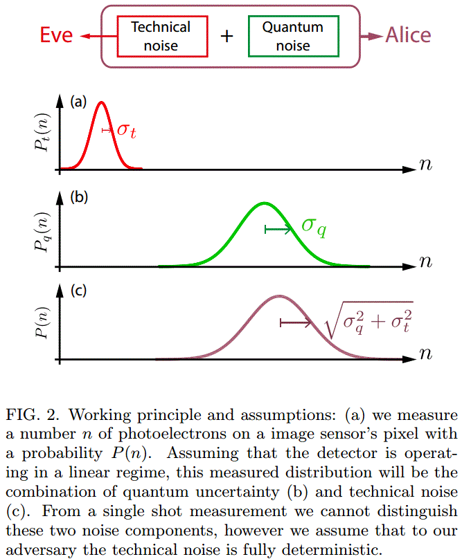
Medium.com: A group of researchers from Geneva University, Switzerland, proposes to use image sensor as a high quality quantum random number generator, widely used in cryptography, security and other applications: "Quantum random number generation on a mobile phone" by Bruno Sanguinetti, Anthony Martin, Hugo Zbinden, Nicolas Gisin. The principle of their work in explained in the figure below. The random number quality has passed a number of tests for randommness.


Thanks to DM for the link!

Omnivision Announces Automotive HDR Sensor and Companion ISP

PR Newswire: OmniVision announces the automotive industry's BSI image sensor and a companion processing chip. The 1.3MP/60fps OV10640 delivers high sensitivity and HDR of up to 120 dB in highly compact automotive-grade packages, while the OV490 enables image and video processing for the next-generation ADAS systems.

"With the consumer predilection for advanced automotive features such as 360-degree surround view, lane departure warning and pedestrian detection, there is a tremendous demand among automobile manufacturers for imaging and processing solutions that deliver exceptionally clear, low-noise images and video," said Inayat Khajasha, senior product marketing manager for automotive products at OmniVision. "The announcement of the OV10640 and OV490 underscores OmniVision's position within the automotive industry as a trendsetter in developing sensors for next-generation ADAS applications."

The OV10640 is the first automotive OmniBSI image sensor, said to have the industry's highest sensitivity. The OV490 is a companion processor that enables simultaneous output of fully processed YUV or RGB data for display-based applications and RAW data for machine-vision downstream processing. The OV10640 and OV490 are now available for sampling, and are expected to complete AEC-Q100 Grade-2 qualification and enter volume production in Q4 2014.

Himax Reports CIS Sales Growth

Himax Q1 2014 earnings report updates on its image sensor business: "Our CMOS image sensors delivered a strong sales growth in Q1, up close to 30% sequentially. Our existing 2 and 5 megapixel CMOS image sensors are producing good sales from select international brands and Chinese white-box customers. However, as noted in the last earnings call, the current shipments comprise mainly of older generation products which are of higher costs. The sales of these products, given their rather significant amount by now, is the key reason why our overall corporate gross margin in the second quarter looks to stay flat or even go slightly down. Without it, our overall gross margin for the quarter would have continued to expand. Maintaining sales of such older generation products is necessary while we are going through design-in process with our customers to replace these products with new designs with much improved gross margins. The new generation products are expected to start shipments in the third quarter.

We expect our 8 megapixel sensors to start shipments later this year, which we believe will contribute to significant sales growth and better gross margin in the second half of the year. Additionally, following multi-year design efforts, we now have a competitive CMOS image sensor product line for automotive and surveillance markets, both large, lucrative and fast-growing markets. This is a market segment with a high barrier of entry where special know-how is required. Collectively, we expect the CMOS image sensor business to more than double in 2014.
"

Himax factsheet says that the company starts to mass produce optics for array cameras in Q2 2014:

Polarization in Thermal Imaging

Optics.org: Polaris Sensor Technologies claims that polarized thermal imaging can offer so much more. David Chenault, the company president, says that their thermal camera with sensitivity to the light polarization, eTherm, is better at seeing at night, better at spotting a potential intruder behind a bush, or to see camouflaged targets. An extra advantage, is that it does not require temperature differences to create an image. "We can form the image from the material itself, from its texture and shape," says Chenault.

Sony Announces 12MP/14.5fps CCD and 8MP/30fps CMOS Sensor

Sony announces 8MP 1/4-inch IMX219PQ CMOS sensor based on 1.12um BSI pixels. The main improvement over its predecessor IMX111PQ is 2x speed, allowing 1080p60 video in 2x2 binning mode:


Sony also launches ICX834ALG (black-and-white) and ICX834AQG (color) 1-inch CCDs with 12.06M resolution. The new CCDs employ the 3.1um EXview HAD CCD II pixel, meaning that they offer a high sensitivity in NIR region. With 4 parallel outputs, the CCDs can achieve 14.5fps speed.

Pixart Q1 2014 Report

Pixart announces its Q1 2014 report. The revenue slightly decreased by 0.1% QoQ to NT$1,198.5M (39.8M USD). Due to favorable change in product mix and the depreciation of NTD, 2014Q1 gross margin was improved to 44.7% from 42.9% in Q4 2013. The operating margin increased to 7.3% from 5.9% in previous quarter. The net income for Q1 2014 was NT$91.8M (3.05M USD). The proportion of optical mouse sensors in the product mix grew to 90%:

Omnivision Explains Image Ghosting Causes

Omnivision's patent application US20140117485 "Negatively charged layer to reduce image memory effect" by Howard Rhodes, Dajiang Yang, Gang Chen, Duli Mao, and Vincent Venezia talks about rarely mentioned but commonly observed ghost image effects: "The electrical signature of an image with high brightness levels that falls onto a complementary metal oxide semiconductor (CMOS) image sensor may remain embedded in subsequently read out electrical signatures of subsequently acquired images. The electrical signature of a previously sensed image remaining in the image sensor has been called a “ghost artifact” or a “memory effect.” This unwanted effect can be exacerbated by repeated exposure of static images, especially high intensity or bright images, to the image sensor. The retention of ghost images represents noise that obscures subsequently acquired images and reduces the signal to noise ratio and may cause blur if there is movement being imaged.

The memory effect problem has been found to be especially present in CMOS image sensors that have been fabricated using advanced fabrication technologies, particularly those employing measures to maximize metal interconnect density. For instance, those fabrication technologies employing so-called “borderless contacts” have been found to be associated with the root cause of this problem.
"

Omnivision explains: "The deposition of the contact etch stop layer is a fabrication technique that may be utilized when providing borderless contacts, which may be employed to increase metal interconnect density in pixel array."

Contact etch stop layer 322 is deposited over passivation layer 320, which is deposited over the pinning surface layers 313 included in example pixel array 302

"In one example, contact etch stop layer 322 may include a silicon nitride based dielectric including for example, silicon oxynitride, silicon carbide, or the like... The mobile charges in the PECVD silicon nitride and/or silicon oxynitride of contact etch stop layer 322 can be moved by electrical forces such as electrical fields placed across contact etch stop layer 322, which can cause unwanted effects in nearby semiconductor regions, such as photodiode regions 312 and/or the pixel circuitry included in the pixels of pixel array 302. For example, the source to drain resistance of a transistor included in the pixel circuitry included in the pixels of pixel array 302 may be affected by the mobile charge in the overlying PECVD silicon nitride of contact etch stop layer 322 by altering the depletion characteristics of an underlying lightly doped source or drain region.

Furthermore, it is noted that net positive charges can be induced directly in the PECVD silicon nitride and/or silicon oxynitride of contact etch stop layer 322 by exposure to visible light that may pass through contact etch stop layer 322, especially when photodiode regions 312 of pixel array 302 are illuminated with bright light when imaging. In particular, the energy associated with the phonon modes of the Si—Si and Si—H crystal structures may participate in the optical excitation of the electrical carriers. Consequently, memory effect is caused by the generation of positive charges in, for example, the SiON film of contact etch stop layer 322 that overlies the photodiode region 312 under the strong light illumination.
"

"To illustrate, FIG. 3A shows light 315 illuminating photodiode region 312, which therefore illuminates and passes through contact etch stop layer 322 as shown. This may occur when photodiode region is capturing an image. As a result of this illumination with light 315, positive charge 317 is induced in contact etch stop layer 322, which induces electrons 319 at the surface of the photodiode region 312 surface as shown.

FIG. 3B shows that after light 315 is no longer present and photodiode region 312 images a darker scene or is in a low light condition after having been illuminated with bright light 315 and after the image has been captured, the induced electrons 319 at the surface of the photodiode region 312 are injected into the photodiode region 312, causing the unwanted memory effect. In other words, when the pixel including photodiode region 312 images a darker scene, the induced electrons 319 at the surface of the photodiode region 312 that were a result of the previously captured image are injected into photodiode region 312, which generates localized dark current causing an unwanted “ghost image” of the previously captured image to appear as a memory effect in pixel array 302.
"

A nice explanation of the positive after-image. Indeed, many CMOS sensors have it positive. In some sensors the after-image is negative though - probably a different effect.
Teledyne DALSA Opens Possibility Hub

Teledyne DALSA Opens Possibility Hub

Teledyne DALSA unveiles Possibility Hub - a content engine for sharing stories and knowledge about imaging technology and its ability to empower human achievement. Continued advances in digital image sensor technology and data processing are driving new and ever more ambitious applications for imaging technology. The Possibility Hub will spotlight these innovations not only in traditional industrial applications, but in the physical and health sciences, arts and entertainment, as well as oceanographic, geographic, and interplanetary exploration.

One of the articles on the Hub "Five CMOS Camera Developments to Watch in 2014" by Eric Fox. The developments are:
  • CMOS Sensors Will Go Big. Real Big. (in resolution and size)
  • CCD + CMOS: The Best of Both Worlds? (TDI implemented in CMOS)
  • Accelerating Speeds and Feeds
  • Better Low-Light Performance
  • More Will Be Happening On-Camera (HDR, ROI, various corrections)