News from France: Sofradir Buys Thales and Sagem IR Sensor Facilities

News from France: Sofradir Buys Thales and Sagem IR Sensor Facilities

Sofradir acquires Sagem and Thales’ IR detector technology development and manufacturing facilities. Under the agreement, Sagem will transfer to Sofradir the Indium Antimonide (InSb) technology. The Quantum Well-Infrared Photodetector (QWIP) and Indium Gallium Arsenide (InGaAs) technologies will be transferred to Sofradir from the GIE III-V Lab, an economic interest group with partners Alcatel Lucent, Thales and CEA.

By consolidating these IR technologies under one roof, Sofradir joins a small circle of IR detector manufacturers with expertise in all the cooled and uncooled IR technologies. Sofradir is currently ranked number one for volume deliveries of IR detectors based on its Mercury Cadmium Telluride (HgCdTe) technology.

"The technologies from Sagem and the III-V Lab enable Sofradir to have from this point forward the complete portfolio of infrared technologies," said Philippe Bensussan, chairman and CEO of Sofradir. "With the new technologies, Sofradir, along with its subsidiary ULIS, will be able to select the technology best adapted to our clients’ applications."
NXP Annouces H.264 IP Security Camera Processor

NXP Annouces H.264 IP Security Camera Processor

Marketwire: NXP announces ASC884xA and ASC885xA series of single-chip video processors for HD IP security cameras. These devices integrate virtually all functions required for an IP camera design -- from raw image sensor data input, ISP, and H.264 compression, to secure encrypted transmission over the network through a Gigabit Ethernet interface.

Capturing 60 frames per second at Full HD resolution (1080p/60), the new series supports H.264 High Profile encoding while consuming less than 1.5 W of power, said to be the best power efficiency and lowest bit rate compared to other solutions on the market today. Further, the ASC884xA and ASC885xA devices incorporate very flexible spatial and temporal (2D/3D) noise reduction for excellent low-light performance.

In addition to ASC8852A flagship product for 1080p/60 performance, NXP is releasing a complete range of pin-compatible Advanced ICs down to 1080p/30 (ASC8850A) and 720p/30 (ASC8848A). The ASC8848A offers an H.264-encoded bit rate of less than 500 kbit/s at a power consumption level close to 0.5 W. Evaluation samples of the ASC8848A, ASC8849A, ASC8850A, ASC8851A and ASC8852A will be available to lead customers starting in Q1 2013, with volume manufacturing starting in Q2 2013.

Sony is the 2nd Best Performing Semiconductor Company in Top 20 List

IHS iSuppli report on top 20 semiconductor companies says about Sony performance:

"After Qualcomm, the next best performance among the Top 20 suppliers is set to be posted by Sony, which will attain 20.1 percent growth in semiconductor revenue. Sony's performance stands in stark contrast to most other major Japanese semiconductor suppliers, whose revenue will collapse by double-digit rates in 2012."

"Sony's strong results are due to its leading position in the image sensor market, which is expected to grow by 19 percent in 2012, with the CMOS image sensor sector of the market seeing its revenue expand by 31.8 percent. Sony's image sensor revenue, which accounts for nearly 60 percent of its semiconductor takings, is expected to expand by 48 percent. Even more amazing, its CMOS image sensor revenues are forecast to more than double," says Dale Ford, iSuppli's analyst.

Invisage Selected as a 2012 Red Herring Top 100 Global Company

Marketwire: InVisage announces that it is a recipient of the Red Herring Top 100 Global award, recognizing the leading private companies from North America, Europe, and Asia.

"This prestigious award reinforces the huge impact our image sensors with QuantumFilm technology will have on the industry at large," said Jess Lee, president and CEO of InVisage. "We appreciate the recognition, and are proud to be part of such an esteemed list of companies."

Update: Invisage web site went through a major redesign and now its technology page shows a small-scale sample image dated by June 28, 2012:

Toshiba Enters Automotive Imaging Market

PR Newswire: Toshiba announces its first image sensor for the automotive and security/surveillance markets, a 1/4-inch TCM5114PL VGA sensor with HDR and fast frame rates.

"Toshiba is leveraging its industry-leading CMOS imaging technology into new markets with stellar results," said Andrew Burt, vice president of the Analog and Imaging Business Unit, System LSI Group at TAEC. "The low-power consumption, and rich imagery enabled by this device in various light conditions will appeal to manufacturers in the automotive industry."

The TCM5114PL sensor delivers DR of 100dB at 60 fps at VGA resolution. The sensor is based on 5.6um pixel with > 6V/lx.s senstivity and has integrated ISP and HDR functions. The TCM5114PL has both a digital and analog (NTSC/PAL) interface so it can connect to currently available display panels. The device supports YUV422/RGB565/ RGB888/ RAW10/RAW12 data formats.

Samples of the TCM5114PL VGA image sensor are currently available. Mass production is scheduled for March 2013. Sample pricing is set at $25.

Sony Production Capacity

Sony Production Capacity

The latest Sony semiconductor business summary sheet dated by Nov. 27, 2012 says that the company's production capacity is 40M units per month for CMOS sensors and 12M units a month for CCDs. The main image sensor fabs are:

  • Nagasaki TEC (CMOS Sensors)
  • Kagoshima TEC (CCDs)
  • Kumamoto TEC (CCD&CMOS Sensors)
  • Sony Device Technology (Thailand) Co., Ltd. (CCD&CMOS Sensor assembly)
IISW 2013 Final Call for Papers

IISW 2013 Final Call for Papers

2013 International Image Sensor Workshop (IISW), to be held on Snowbird Resort, Utah, USA, June 12-16, 2013, published a Final Call for Papers:

The scope of the workshop includes all aspects of electronic image sensor design and
development. In addition to regular papers, the workshop will include invited talks, poster presentations, discussion sessions, and Walter Kosonocky Award. Extra time has been added to permit longer discussion and more informal meeting time.

Papers on the following topics are solicited:

Image Sensor Design and Performance

  • CMOS Image sensors, CCD and CID image sensors. New architectures.
  • Image sensors with rolling shutter and global shutter.
  • Image sensors architecture, Low noise readout circuitry, ADC designs
  • High frame rate Image sensors, High dynamic range sensors, Low voltage and low power
  • High image quality. Low noise. High sensitivity. High color reproduction.
  • Non-standard color patterns with special digital processing
  • System-on-a-chip, Image sensors with digital preprocessing

Pixels and Image Sensor Device Physics

  • New devices and structures. Advanced materials.
  • Small pixels development, testing, and characterization
  • New device physics and phenomena
  • Techniques for increasing QE, well capacity, reducing crosstalk, and improving angular performance
  • Front side illuminated and back side illuminated pixels and pixel arrays
  • Nanotechnologies for Imaging
  • Pixel simulation: Optical and Electrical simulation, 2D and 3D, CAD for design and simulation.

Application Specific Imagers

  • Image sensors and pixels for depth sensing: TOF, RGBZ, Structured light, etc.
  • Image sensors with enhanced spectral sensitivity (NIR, UV)
  • Pixels and Image sensors for stereo Imaging
  • Sensors for DVC, DSC, Mobile, DSLR and mirror-less cameras
  • Array Imagers and sensors for Computational Imaging
  • Sensors for medical applications, microbiology, genome sequencing,
  • High energy photon and particle sensors (X-ray, Radiation).

Fabrication and testing

  • New fabrication techniques. Backside thinning. Scaling.
  • Wafer stacking, multilayer sensors, “3D” integration
  • Advanced optical path, Color filters. Microlens. Light guide
  • Packaging and Testing. Wafer level cameras
  • Reliability. Yield. Cost.
  • Defects. Leakage current. Radiation damage.

Submission of papers: Abstracts should be submitted electronically to the Technical Program Chair, Gennadiy Agranov (see email in the pdf on IISW site). The deadline for abstracts submission is January 23, 2013.

8MP Stacked Sensor, 12MP Power and Speed Marvel and More From Sony

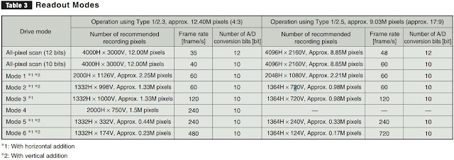
Sony Cx-News vol. 70 is entirely devoted to new and very impressive image sensor announcements. The first of the two most interesting ones is 1.55um BSI pixel-based IMX117CQT. This 1/2.3-inch 12.4MP sensor is an improvement on the similar but older IMX078CQK. The new sensor is faster, lower power, has wider light acceptance angle, and more:


The sensor is very fast delivering 35fps at full resolution at 430mW power. It also capable to 4K/60fps video (10b ADC mode) and includes HD-ish slow motion modes:


Another important announcement is the first stacked sensor product, the 1/4-inch 8MP 1.12um pixel ISX014, naturally, with integrated ISP:

Sony illustration of the stacked structure does not seem to have
any wafer-to-wafer contacts in the pixel array area

Not much information is given about the sensor. It supports 1940 x 1080p video at 30fps and 1280 x 720p video at 60fps. The built-in scalar function makes it possible to shrink all of the 8MP to perform 16:9 cropping for video. Power consumption is 270 mW in 8MP JPEG@15fps mode or 202 mW in 2MP YUV@30mode which are quite good numbers, possibly due to an advanced process node used for ISP die.

The image samples which were supposed to show the sensor's high quality, are of low resolution, unfortunately:


Another announcement is the new 1-inch 9.19MP CCDs: the ICX814ALG (B&W) and the ICX814AQG (color). The sensors have 4 outputs and multitude of readout modes, the fastest one being 1080p at 36fps:

 Raymond Wu Re-Joins Omnivision

Raymond Wu Re-Joins Omnivision

PR Newswire: Omnivision reported its quarterly results on the higher end of its guidance: $390.1M, as compared to $258.1M in the previous quarter, and $217.9M a year ago. GAAP net income $10.3M, as compared to $2.3M in the previous quarter, and $21.1M a year ago.

GAAP gross margin is 16.6%, as compared to 19.1% in the previous quarter and 30.6% a year ago. The sequential decrease was attributed to an increase in shipment mix of advanced products that carried high manufacturing costs.

"In addition, I am pleased to announce the addition of Raymond Wu to OmniVision's management team," said Shaw Hong, Omnivision's CEO. "Raymond, one of our co-founders, has agreed to re-join us as our President, effective December 1, 2012. During his previous tenure, Raymond's intellect, experience and influence extended to market development, engineering and sales. We are enthused by his return, and with his knowledge of our company and the industry, I expect Raymond to make significant contributions to OmniVision's continued growth in the years to come."

Raymond Wu used to be Omnivision's EVP and left the company in August 2006.

Update: SeekingAlpha published Omnivision's earnings call transcript with more details on its business.

PMD and Mesa ToF Cameras Comparison

Open access Remote Sensing journal published a nice paper comparing PMD's CamCube3.0 and Mesa Imaging's SR-4000 ToF cameras and also giving a nice background on other ToF solutions:

SR-4000 and CamCube3.0 Time of Flight (ToF) Cameras: Tests and Comparison
Dario Piatti and Fulvio Rinaudo
DITAG, Politecnico di Torino, Torino, Italy

The paper starts with a nice table filled with parameters of many ToF cameras, both historical and available now on the market:


The influence of camera warm-up on distance measurement is analyzed: a warm-up of 40 minutes is suggested to obtain the measurement stability, especially in the case of the PMD's CamCube3.0. Depth accuracy tests have shown similar numbers of of order of millimeters for both cameras.

Mesa's SR-4000 is on the left, PMD's CamCube3.0 on the right.
Question mark means the accuracy has not been measured yet.

Via Vision Systems Design.
Pansonic Presents its SmartFSI at IDW 2012

Pansonic Presents its SmartFSI at IDW 2012

International Display Workshops combined with Asia Display 2012 to be held in Kyoto, Japan on December 4-7, has few image sensor presentations. For the first time Panasonic openly presents its SmartFSI technology:

Evolution of Eyes and Image Sensors
H. Watanabe
Panasonic, Japan

The evolution of the eye and image sensors was overviewed. The possible disadvantage of the inverted structures of human eyes and FSI image sensors was solved with the use of the lightpipe function. A novel “SmartFSI” image sensor with stacked lightpipe structure demonstrated a high performance.

There are quite a few other interesting presentations, including 3 by Samsung:

A 1.5 Mpixel RGBZ CMOS Image Sensor for User Interface and 3D Image Capture
W. Kim, J. Yun, S.-H. Lee, Y. Wang, I. Ovsiannikov, Y. Park, C. Chung
Samsung, Korea, USA

A 1.5 Mpixel RGBZ image sensor to capture color (RGB) and depth (Z) at the same time is presented. Time-Of-Flight (TOF) method is used for depth. Color pixels and depth pixels are placed together in pixel array with specially designed RGBZ pattern. It demonstrates excellent depth performance and full color image.

A Full-HD CMOS Image Sensor with TimeMultiplexed 2D/3D Image Acquisition
S.-J. Kim, J. Shin, J. D. K. Kim, B. Kang, K. Lee
Samsung Advanced Inst. of Tech., Korea

We present a 1920x1080 pixel array to provide high-resolution 2D color images and high-accuracy 3D depth maps in a time-multiplexed manner. The prototype chip demonstrates the demodulation of 20 MHz time-of-flight signal with the contrast of 52.8%, achieving less than 38 mm depth error between the distance of 0.75 m and 4.5 m. [For a good multi-purpose gesture recognition one needs less than 10mm accuracy - ISW]

Amorphous Oxide Semiconductor Thin Film Transistor for Novel Device Applications
S. Jeon, I. Song, S.-E. Ahn, C. I. Kim, U.-I. Chung
Samsung Advanced Inst. of Tech., Samsung Elect., Korea

Among various semiconductor devices, electronically active oxide thin film transistors (TFTs) have received considerable attention for a wide range of device applications. In this presentation, we review various device applications utilizing amorphous oxide semiconductor TFT, which include photo-sensor, image sensor and other device applications.

Low Noise Readout Circuits Interface Using a Capacitive-Feedback Frontend Amplifier for High Output Impedance Sensors
K. Mars, S. Kawahito
Shizuoka Univ., Japan

In this paper a low-noise high-gain readout circuit interface for high output impedance sensors is presented. Theoretical noise analysis and simulation results shows that by using a high-gain switched capacitor amplifier, the thermal noise is greatly reduced if the dominant reset noise component at the charge summing node is canceled.

An Ultra-Low Voltage CMOS Imager with Novel Pulse-Width-Modulation Readout
C.-C. Hsieh, M.-T. Chung
Nat. Tsing Hua Univ., Taiwan

A 0.5 V PWM CMOS Imager chip with threshold variation cancelling and programmable threshold control scheme was implemented. It achieves 0.055% pixel FPN, 0.65 LSBrms random noise at dark, and 82 dB dynamic range at 11.8 fps. The chip consumes 4.95 µW at 11.8 fps; results in a iFOM as 163.9 pW/f-p.

Discussing Pixel Circuits for Hybrid Sensor and Display Pixel Arrays
N. Papadopoulos, M. Yang, M. Esmaeili-Rad, M. Sachdev, W. S. Wong
Univ. of Waterloo, Canada

The hybrid sensor and display pixel proposed consists of: light sensor and integrated display onto the backplane. Phototransistors incorporating both sensing and switching on the same device was used. The backplane was implemented using a driving TFT and an OLED. The grey scale is generated by pulse-height and width voltage modulation.

Advantest Upgraded its CIS Tester Speed

Advantest introduces what it claims to be the industry's fastest image-capture module to cost-efficiently test image sensors with D-PHY and M-PHY interfaces. The new T2000 3Gbps CMOS Image Capture Module operates on its T2000 ISS system:


The T2000 3Gbps CMOS Image Capture Module simultaneously tests up to 64 devices in parallel, significantly reducing test costs. In addition to improving yields by performing at-speed testing in production, the module also can be used to shorten turnaround time in verifying semiconductor designs on first silicon.


"Ongoing, rapid improvements in the performance and resolution of CMOS image sensors as well as the growing volume of electronic products depending upon them continue to exert downward pressure on production costs," said Satoru Nagumo, senior vice president of the ASD Test Business Group at Advantest Corporation. "Our newest generation of image-capturing technology enables our customers to lower the cost of test while meeting the performance requirements for advanced image sensors."

Toshiba Announces 1.12um BSI Sensor with Improved SNR

PR Newswire: Toshiba announces a 13MP, 1.12um pixel sensor claimed to deliver high-image quality equivalent to a 1.4um pixel. The new T4K37 feature BSI and integrated color noise reduction (CNR) and fits into an 8.5mm x 8.5mm size camera module.

The miniaturization of pixel size impacts performance of light sensitivity and SNR in today's 1.12um pixel image sensors. BSI technology helps improve sensitivity, but is said to fall short on elevating image quality. Toshiba developed its newest image sensor with BSI and CNR integrated on the sensor to address both low-light sensitivity and SNR. As a result, the Toshiba CMOS image sensor provides approximately 1.5 times higher SNR than a 1.12um pixel sensor with no CNR.

Samples of the new Toshiba sensor, the T4K37, will be available in December 2012. Sample pricing begins at $20.00.


Update: It appears that Japanese PR has much more info. Among the pictures, it shows the CNR effect:


Here is the Google translation of CNR principle:

"CNR Our circuit has adopted the type to compare the image between frames by a digital filter circuit to suppress the color noise, without compromising a sense of resolution, of 1.12 micrometer pixel circuit not installed CNR SN ratio of about 1.5 times to accomplish, to achieve the SN ratio of the pixel corresponding to 1.4 micrometers."

The sensor is fast, it delivers 30fps at full 13MP resolution. The Japanese PR also has a table with two other sensors, apparently based on the same 1.12um pixel:


Update: Toshiba published a product page of the 1/3.07-inch T4K37 sensor. The block diagram shows a location of Color Noise Reduction part (CNR). The output format is either 8b or 10b.

ON Semi and Teledyne Designed 16MP MCT Sensor

ON Semi and Teledyne Designed 16MP MCT Sensor

Business Wire: ON Semiconductor collaborated with Teledyne Imaging Sensors to manufacture an Extremely Large Stitched Read Out Integrated Circuit (ELS ROIC) for astronomy.

The 16MP H4RG-15 consists of Teledyne’s HgCdTe detector material hybridized to a CMOS readout circuit. It is said to be the largest sensor ever produced for IR astronomy. The H4RG-15 63 mm x 63 mm stitched CMOS ROIC uses ON Semiconductor’s proprietary 180nm process. The ROIC is so large that only four die fit onto a 200 mm wafer.

The H4RG-15 ROICs were manufactured at ON Semiconductor’s fab located in Gresham, Oregon. With this project, ON Semiconductor has demonstrated that it can successfully produce the H4RG-15 with the yield required for this next generation sensor.

The H4RG-15 sensor has been installed at the University of Hawaii’s observatory on Mauna Kea to confirm the performance of the sensor under telescope observing conditions. "The resolution with which images can be captured using this new sensor system represents a major step forward in the progression of IR astronomy," said Dr. Donald Hall of the Institute for Astronomy at the University of Hawaii, who is the principal investigator for the NSF-funded H4RG-15 development program.

Samsung S5K3H5 CMOS Sensor Promo

Samsung published a Youtube promo of its 8MP, 1.4um pixel S5K3H5 sensor promo. The sensor is used in Samsung Galaxy S3 smartphone. The video goes through the sensor spec with the video illustrations in the background. Another feature of the video is the 1.9MP 1/6-inch 1.75um pixel front sensor S5K6A3:

Leap Motion's Demos on Youtube

There are few new Leap Motion's gesture control videos appeared on Youtube. The videos are from different third party developers that Leap Motion kindly collected into a single playlist.

The first one shows finger recognition in action. The room is quite dark, hopefully it's not a system limitation:


The Quadrotor control works quite nicely. A delay is noticeable but it might come from mechanical stuff:


The pong game gesture control is shown in dark room too:

IS2013 Publishes Confirmed Speakers List

IS2013 Publishes Confirmed Speakers List

Image Sensors 2013 conference to be held on March 19-21, 2013 in London, UK, published an impressive list of confirmed speakers:
  • Dr Howard E Rhodes, CTO, OmniVision, USA
  • Prof Franco Zappa, PoliMI, Italy
  • Dr G Humpston, Director of Applications (Europe), Digital Optics Corporation, UK
  • Dr.Ir Peter Centen, Director R&D, BU Cameras Grass Valley, The Netherlands
  • Prof Edoardo Charbon, TU Delft, The Netherlands
  • Paul Danini, Technology & Market Analyst, Imaging Technologies & Mems Devices, Yole Developpement, France
  • Dietmar Wueller, Director, Image Engineering, Germany
  • Dr Gerhard Holst, Head of R&D, PCO, Germany